Title here
Summary here


Up to 100Gbps per port, on a wide range of FPGA dev boards
May 28, 202611 minutes

In this post I want to tell you about our latest-and-greatest new product: the 2x QSFP28 FMC. This is an FPGA Mezzanine Card (FMC) with a high-pin-count (HPC) connector and as the name suggests it has 2 QSFP28 cages for mating with QSFP/QSFP+/QSFP28 modules. Each QSFP28 cage connects to four gigabit transceiver lanes and supports up to 28Gbps per lane - that means that each cage can support an aggregated link speed of up to 100Gbps.
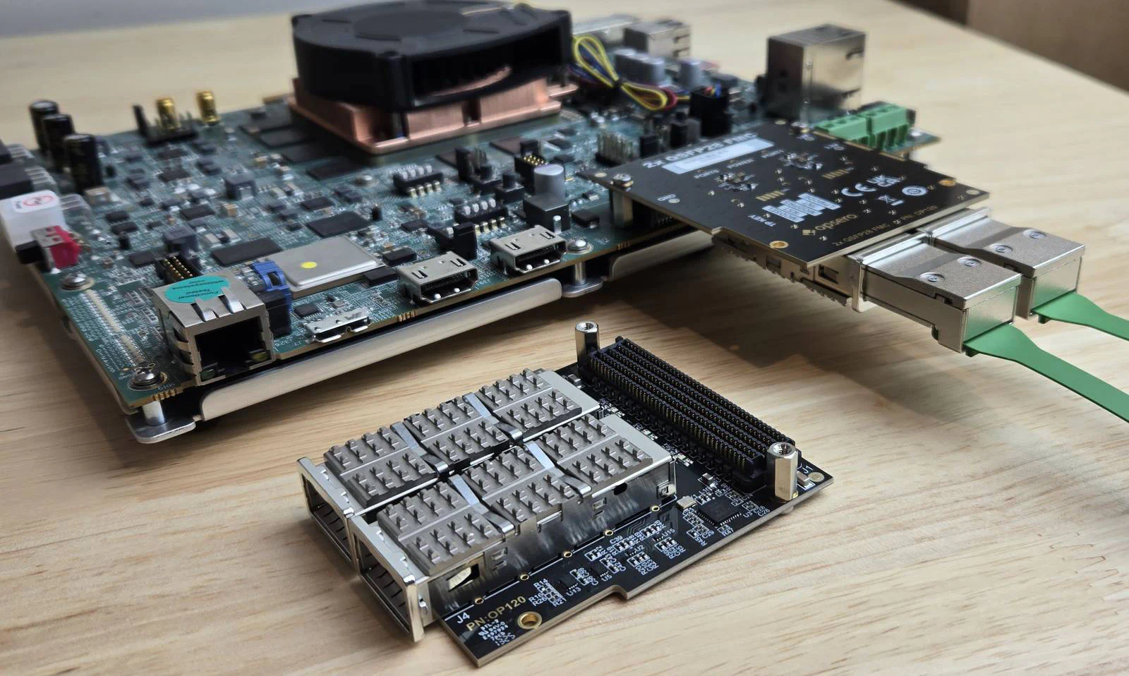
This was the test setup we used to do our IBERT testing - more on that further down. On the top side of the board we put the QSFP28 cages and all of the active components. Most of the ICs are level translators, but there is also a jitter-attenuating clock multiplier (Si5328) and its 114.285MHz crystal. It has a 3.3VDC switching regulator that provides power to the QSFP28 modules derived from the 12VDC input from the FMC connector. If you want a labelled view of which part is which, just check out the detailed description page of the datasheet.
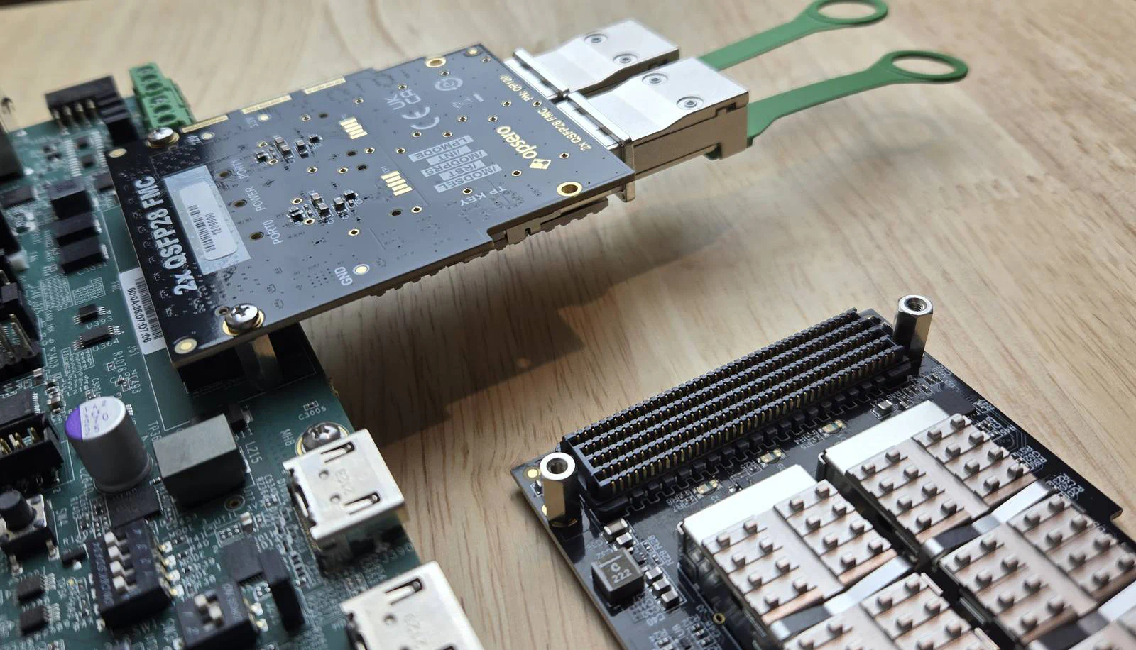
The bottom side is where we put most of the labelling, the test points and the bicolor user LEDs. The LEDs are bottom-entry parts but they’re soldered on the top side of the board. I like to keep as few parts as possible on the bottom side of the board so that there’s less chance of them breaking off if the card gets dropped or something falls on it (not a rare occurance on the typical cluttered desk of an electrical engineer).
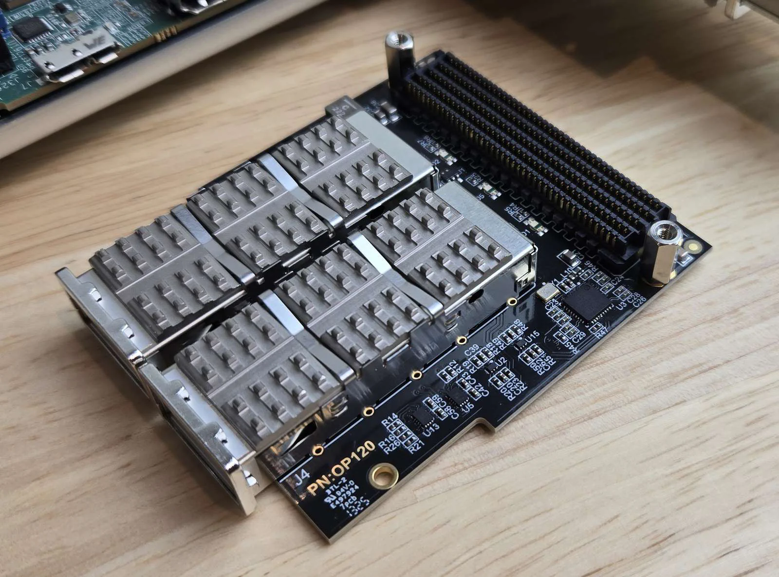
The image above gives you a closer look at the top side. You can see the 2x QSFP28 cages, the high pin count FMC connector, and the supporting circuitry between them.
Here’s a quick summary of the features:
The FMC connector provides power and presents the following I/O to the FPGA: 8 gigabit serial lanes (4 per port), QSFP management I/O (MODPRS_L, RESET_L, LPMODE, INT_L, MODSEL_L), I2C buses for the EEPROM, each QSFP module and the clock multiplier, an LVDS recovered clock from the FPGA into the clock multiplier, an LVDS configurable clock back out, a clock loss alarm, and the drive signals for the user LEDs.
One thing worth pointing out: the 2x QSFP28 FMC needs 8 gigabit transceivers to support both ports (DP0-DP7), so it requires a high pin count (HPC) or FMC+ connector. Low pin count (LPC) connectors only route a single transceiver (DP0) - they won’t work with this board. If your carrier only has DP0-DP3 routed on its HPC, you’ll still be able to use Port 0.
Here are a few application ideas that we designed this for:
This is the second Opsero product designed for 28Gbps serial links (the first was the Quad SFP28 FMC) and this time we put even more effort (and expense!) into getting the signal integrity where it should be (see the lessons learned below). By the way, 28Gbps is pretty much the limit of these FMC connectors, so they’re useless for AMD Versal Prime 112Gbps (PAM4) GTM gigabit transceivers - but I’m going off track. A quick summary of the choices:
If you want the full reasoning behind these choices, my Quad SFP28 FMC post goes into more detail and points to the DesignCon papers that we leaned on.
The proof is in the eye diagrams. Simulations are nice but when you make physical products, they have to actually work.
We ran IBERT on the VCK190 development board with the 2x QSFP28 FMC and a pair of QSFP28 loopback modules plugged into both cages. Each lane was driven with a PRBS31 pattern at 28Gbps, error free.
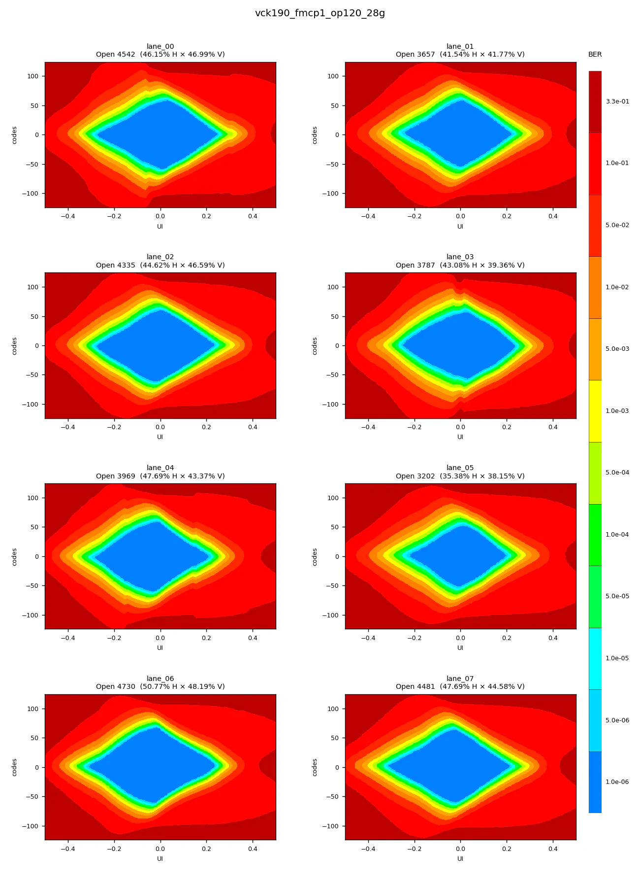
Wide open eyes on all 8 lanes at 28Gbps. We’ve also tested this on the VEK280, and we have customers using it on other target boards already.
We’ve verified compatibility for the 2x QSFP28 FMC on quite a few AMD/Xilinx development boards including:
What I mean by “verified” is that we’ve made sure that those boards satisfy all of the requirements of the FMC card, including VADJ voltage, and GT and I/O pin assignments as well as mechanical constraints. Hardware tests have so far been limited to VCK190, VEK280 and ZCU216 but when we get the ref design up-and-running, that list will grow longer.
On the boards with FMC+ connectors and 28Gbps-capable transceivers (the RFSoCs and the Versal boards), you can hit the full 2x 100G. On the HPC carriers limited to 10Gbps transceivers, you’ll still get 2x 40G, which is still a good deal of bandwidth.
The full table with notes, supported port counts and link speeds is on the compatibility page of the datasheet. We’ll be releasing reference designs for these boards over the coming months.
Getting a new product designed, built and put on the market is not always easy. I like to share the stories and the lessons learned when I can.
If you’re connected to me on LinkedIn, you may have noticed that I started sharing photos and making announcements of this product early last year - so what happened? Problems happened.
The first prototypes looked good. Up to 10Gbps per lane, they were good. However, when we pushed it up to 28Gbps, bit errors started to appear, and two lanes completely dropped out. Clearly, we had a signal integrity problem.
After breaking-out from the pins, drop to the inner layers as soon as you can. Actually I already knew about this best-practice from one of Don Telian’s DesignCon papers, but I didn’t take it seriously enough (obviously). So Don’s reasoning is that the outer copper layers of the PCB have a “roughness” to them that the inner layers don’t have. This roughness improves component adherence - but it also contributes to losses on high frequency traces. The inner layers are smoother and less lossy, so use them for the large majority of the trace path. But this wasn’t the cause of my problem.
In my case, those two lanes, that “completely dropped out” at 28Gbps, were traces that I had extended on the top layer into a region where the QSFP28 loopbacks had a metallic lip that hovered just above the surface of the PCB. Those traces (microstrips) were designed for 100 ohm differential impedance and the dimensions are calculated with the assumption that they have open air above them - not metal. Basically this metal lip was changing the impedance of those traces in that small section and causing a significant discontinuity at 28Gbps, hence reflections and the lanes dropping out. I broke the metal lips off - the lanes came up.
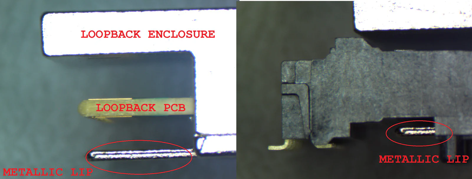
The image above shows two photos: on the left, a profile shot of the QSFP28 loopback module showing the protective metallic lip; on the right, the same profile shot but of the QSFP28 module plugged into a socket.
So I would add to Don Telian’s guidance by saying that you shouldn’t route too far on outer layers because you can’t always control what goes on up there - maybe there’ll be a wire harness sitting close to your traces, maybe you’ll need a heat-sink or a shield in that area later, who knows? On inner layers you can control what is above and below your traces; on outer layers you cant, and anything that gets too close to those traces can significantly change its characteristics at these frequencies.
So with a re-spin I could fix the worst two lanes. Great. But I still had bit errors to clean up on the other lanes. I needed EM simulation and advice from a signal integrity expert.
I took this problem to E3 Designers, a company that was highly recommended to me. I spoke with Dan Binnun, the lead designer and SI specialist. Dan analysed the key elements: the PCB stackup, the skew compensation (P/N length matching), the transitional vias, the QSFP28 socket and the FMC connector. He came back to me with detailed recommendations for how to design the skew compensation, the transitional vias, and the escape routing for each connector. All of these recommendations were backed up by Ansys EM simulations.
Here are some of the layout improvements that led to a single successful re-spin and our stunning IBERT results above:

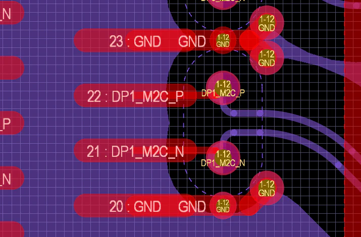
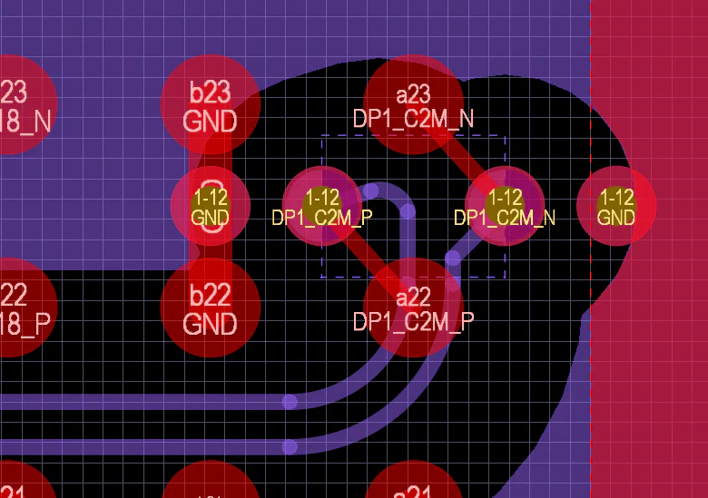
The message that I want to convey here is: be careful at 28Gbps+ because tiny details can come back to bite you. In fact, Dan would say that you should be simulating for even lower speeds, like 16Gbps. At these frequencies, leaning on best practices might not be enough, and you’ll likely save yourself some time and money by working with a company like E3 Designers before the layout even begins.
The 2x QSFP28 FMC is available directly from the Opsero website. It’s also listed at Digi-Key - the initial Digi-Key stock sold out quickly, but more stock will be coming online next week.
As always, if you have any questions about the board, compatibility with your carrier, or anything else, feel free to reach out.