Title here
Summary here
Now With Host and Device Mode in One Board
April 16, 20265 minutes

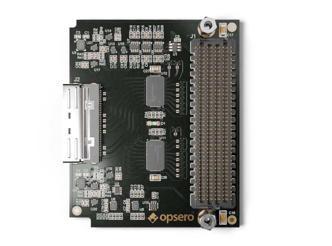
Last year I released the MCIO PCIe Host FMC (OP100), a board designed to connect U.2 NVMe SSDs and other PCIe devices to FPGA development boards via MCIO cables. Notice the word “Host” in the product name. The original plan was to follow up with a companion product – the MCIO PCIe Device FMC – which would let you connect to MCIO hosts such as server motherboards, and also enable setups where two FPGA boards with FMC connectors could be linked together, one as the host and the other as the device.
While working on the device-side design, I realized that with high-speed differential MUX/DEMUX
chips we could build a single board that supports both host and device mode, selectable at
runtime via a single FMC I/O pin we call HOST_MODE_N. Rather than ship two separate products, I
decided to discontinue OP100 and replace it with the
MCIO PCIe FMC (OP103) – one board that satisfies
both needs.
The OP103 opens up a range of configurations that were previously difficult or impossible with a single FMC mezzanine card:
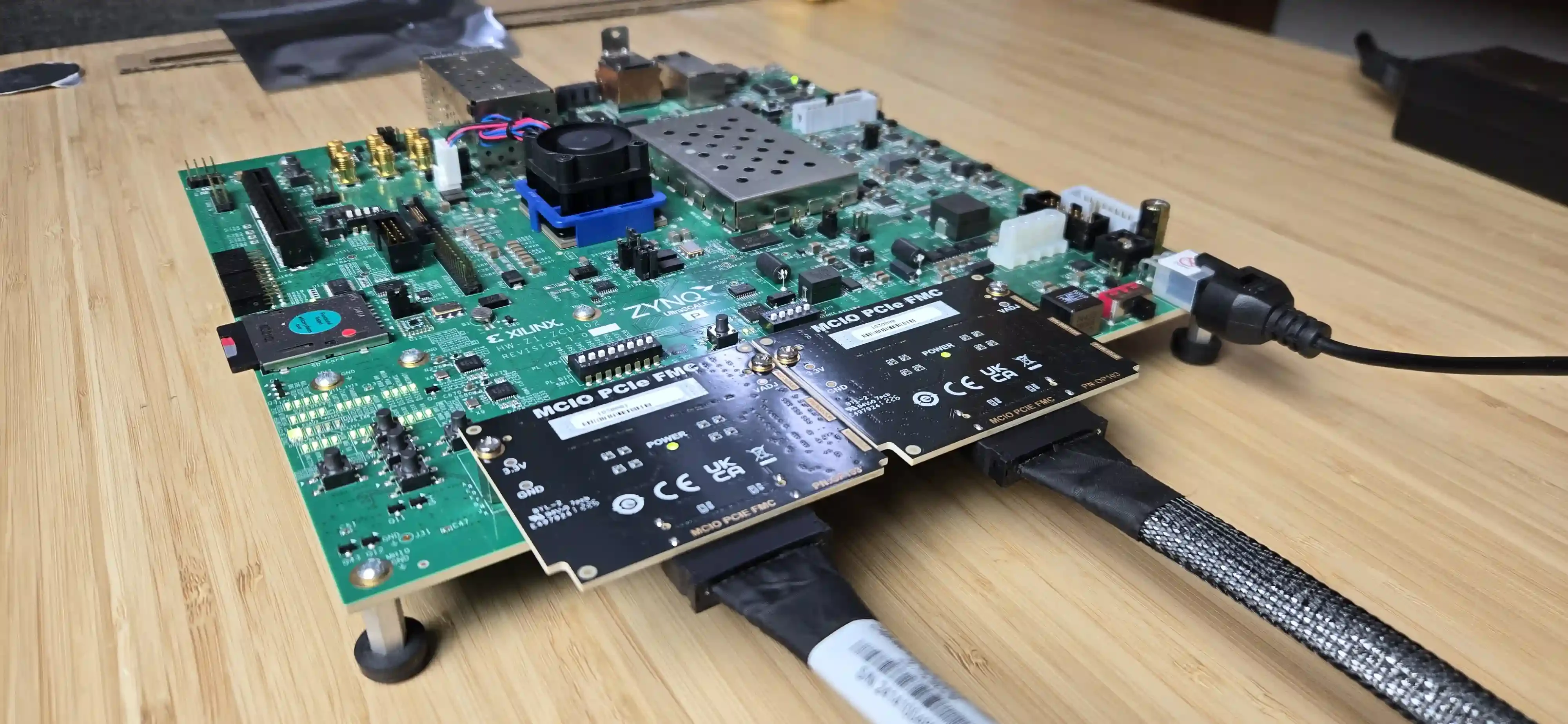
The production test for this product is unique so I thought I’d share a few details. Most Opsero FMC products are tested one at a time, with the FMC card DUT plugged into a test bench, usually a dev board like the UltraZed-EV Carrier. The test code programs the EEPROM with the correct IPMI data and then runs a series of tests to check all of the critical paths on the board and make sure that there are no assembly defects. In the case of the OP103 we actually test two boards at a time. The test setup uses a Xilinx ZCU102 evaluation board with two OP103 boards plugged into the HPC0 and HPC1 FMC connectors, linked together via an 8-lane MCIO cable (see image below). This dual-FMC loopback configuration lets us test the board in both host and device modes by swapping roles between phases.
The test runs in two phases – first with HPC0 as host and HPC1 as device, then the reverse – and checks:
CPRSNT_N, PERST_N, MCIO I2C) when the SB_DISABLE line is asserted. It’s actually thanks to the
switches that it is able to support both host and device modes. The test drives
each signal from one side and reads it on the other, confirming propagation when the switch
is enabled and isolation when it’s disabled.LOCAL_CLKS_N actually switches the clock source by confirming that
GT lanes fail when the local oscillator is deselected.As with all of our FMC products, the production test UART output displays all of the test results and this is logged and saved for future reference.
To characterize the signal integrity of the OP103 at speed, we ran 2D eye scans on all 8 GT lanes at 16 Gbps using PRBS-31. The test was performed on a VCK190 evaluation board with a passive loopback attached to the MCIO connector providing 1:1 lane-to-lane loopback.
The combined results for all 8 lanes are shown below:
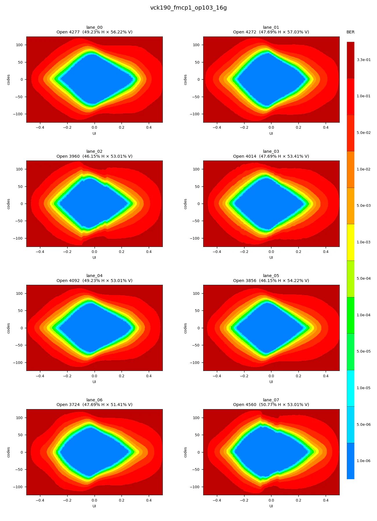
All 8 lanes are locked, error free and showing healthy, open eyes.
These results were generated using our open-source opsero-fmc-ibert project, which includes ready-made IBERT designs for several Opsero FMC products targeting VCK190 and VEK280 evaluation boards. The project includes an automated test script that programs the FPGA, brings up the IBERT links, runs eye scans on every lane, and saves the results.
A companion script renders the Vivado eye-scan CSVs into PNG images using the same discrete 12-colour BER scale that Vivado’s Hardware Manager uses, so the results are immediately recognisable.
The MCIO PCIe FMC (OP103) can now be purchased from the Opsero website:
You can also get it on Digi-Key here:
Digi-Key - Opsero MCIO PCIe FMC (OP103)
Full documentation – including pinout, schematic reference, mechanical drawings, and application notes for host and device mode – is available on our docs site: