Title here
Summary here


A Universal MIPI Camera FMC Proof-of-Concept
September 21, 202612 minutes

Note: This article was first published in Issue 2 of the FPGA Horizons Journal in January 2026. It’s getting a second life today because I’ve just released the source code: MIPI over Chip2Chip. Anyone can now reproduce the setup and receive 1080p video from two Raspberry Pi cameras over a 10Gbps serial link.
Vision has always been one of the most compelling and natural application areas for FPGAs. Their ability to perform massively parallel computations and interface directly with high-speed image sensors makes them ideal for real-time image processing. Yet, despite these strengths, when it comes to rapid prototyping and experimentation, it is still difficult to find modular solutions for connecting FPGAs to image sensors.
In an ideal prototyping or proof-of-concept scenario, a developer could simply pick an FPGA board and an image sensor and connect them through a standard interface. While many FPGA platforms can interface with USB cameras - often sufficient for low-bandwidth applications - most vision systems demand a higher-performance link. For these, the MIPI CSI-2 interface is often the preferred choice.
MIPI CSI-2 has become the most widely used interface between image sensors and FPGAs. It delivers high-bandwidth pixel data over just a few differential pairs, making it ideal for compact, high-speed camera links. Each lane can run at multiple gigabits per second, and with up to four lanes per sensor, CSI-2 can easily support multi-megapixel, high-frame-rate video streams. Its low pin count, excellent signal integrity, and broad sensor compatibility have made it the standard for everything from smartphone cameras to industrial vision modules.
I’ve long felt that there should be an FMC-based solution for connecting MIPI CSI-2 image sensors to FPGA development boards. A few options do exist - including our own RPi Camera FMC - but these are essentially custom designs, each tied to one or two specific carrier boards rather than being broadly compatible. This runs counter to the goal of the VITA 57.1 FMC standard which was to modularize I/O and make hardware interchangeable across platforms.
So why isn’t there a universal MIPI CSI-2 FMC on the market? The answer lies in pin restrictions. The AMD MIPI CSI-2 Rx IP, and equivalent implementations from vendors such as Altera and Lattice, require specific FPGA pins that support the electrical and timing characteristics of the MIPI D-PHY interface. The FMC standard, while it defines the locations and electrical specifications for I/Os, clocks, gigabit transceivers and power supplies, it does not constrain pins at the level of the byte-group or specialized functions which are important for MIPI implementations (eg. DBC, QBC in AMD UltraScale/UltraScale+ devices). As a result, one can design a MIPI CSI-2 FMC to match one or two FPGA carriers, but it’s impossible to assign the pins to make it broadly compatible.
Our idea is to break that limitation by adding a small FPGA directly on the FMC card. This way, the MIPI CSI-2 pin assignments are fixed and can be chosen to suit the mezzanine card’s FPGA. On the other side, the interface with the carrier board’s FPGA can be a general-purpose, easily reproducible link – such as Aurora – ensuring compatibility with a wide range of carrier boards. The image below illustrates the concept. For this example we have chosen the Artix UltraScale+ for the mezzanine FPGA and two Raspberry Pi cameras for the MIPI CSI-2 image sensors.
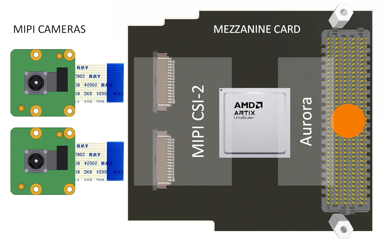
This architecture not only solves our compatibility problem but also comes with an added benefit: the mezzanine FPGA provides more resources that can be used for image processing, freeing up resources on the carrier board. To provide an example, a basic video pipe for a single MIPI CSI-2 image sensor can require 20,000 LUTs, 20,000 registers and 40 BRAMs – and these numbers can grow exponentially when we need to support higher resolutions, frame rates or more complex processing. By offloading the video pipe to the mezzanine card, either partially or fully, the main device can dedicate more resources to higher level functions such as AI inference.
The diagram below illustrates a typical video pipe that might be implemented in the mezzanine FPGA. It starts with a MIPI camera on the left and ends with the FMC connector on the right. The video pipe contains the basic elements that convert the MIPI camera’s RAW10 output to an AXI-Stream of RGB pixels, a preferred format for processing images in an FPGA.
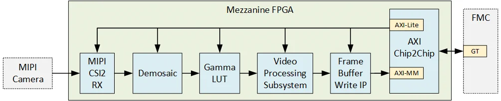
To allow the carrier board’s FPGA to configure and control these processing blocks, we use the AXI Chip2Chip IP core. This IP enables an AXI4-Lite interface to be tunneled between the two FPGAs over a serial Aurora link, effectively extending the control bus across the FMC connection.
At the end of the video pipeline, a Frame Buffer Write IP typically stores pixel data into DDR memory. In our design, that DDR memory resides on the carrier board, not the mezzanine. Once again, the AXI Chip2Chip IP bridges this gap by passing an AXI4 Memory-Mapped interface across the same Aurora link, allowing the mezzanine’s video pipeline to write directly to the carrier’s memory subsystem.
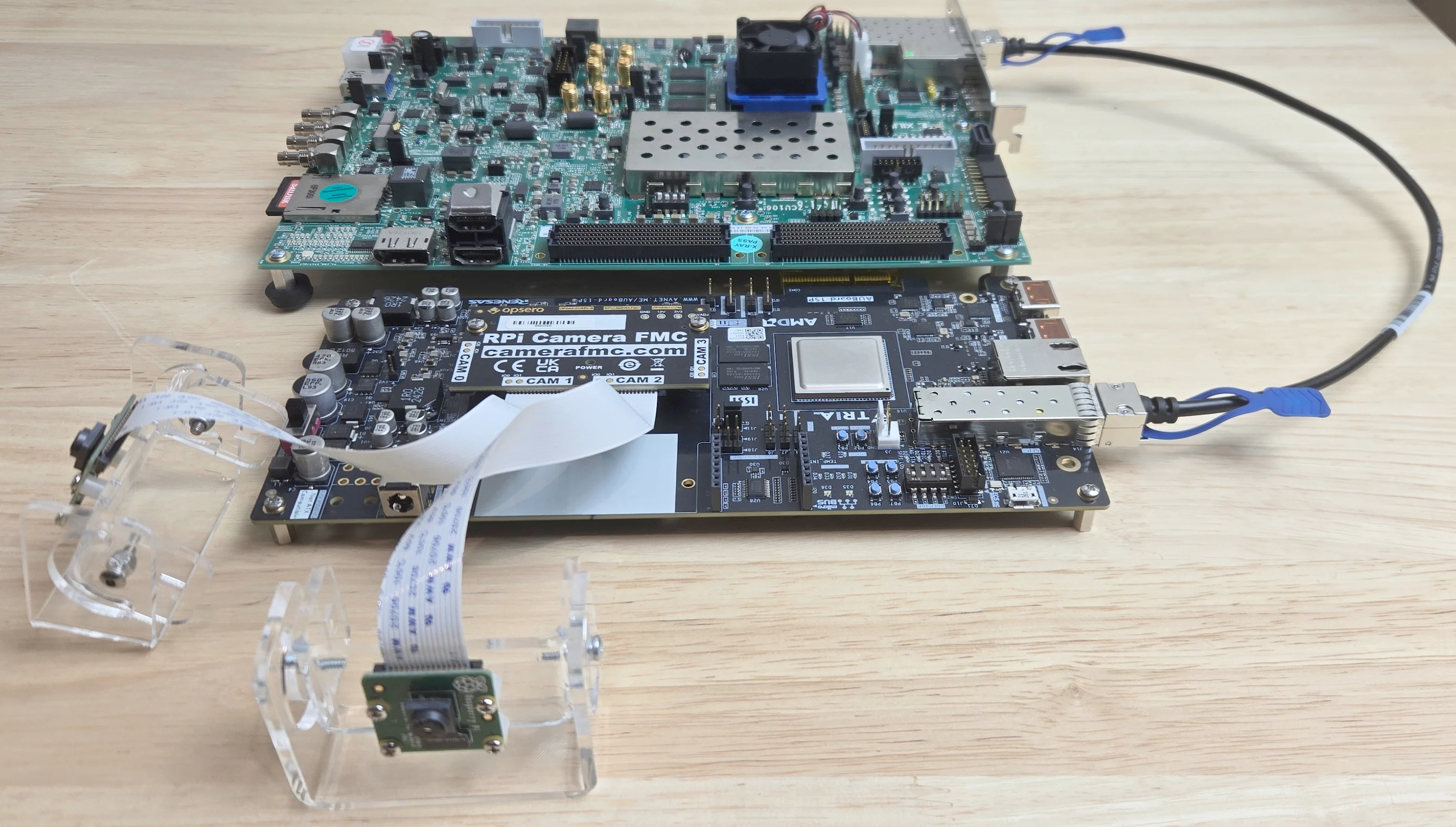
As with any new product development, it is always best to make some effort to prove that the concept will work as expected. To do that, we built a demonstration platform with the AMD ZCU106 serving as the main board and the Tria AUBoard standing in for the mezzanine card. The AUBoard hosts our RPi Camera FMC, allowing us to connect two standard Raspberry Pi cameras. The Aurora serial link was implemented over an SFP+ DAC cable connected between the two boards. The setup is shown in the photo below.
In our effort to design a truly universal MIPI CSI-2 FMC, we now have most of the hardware architecture defined and we even have a prototype to help us to prove the concept. But one important question remains: how do we make the main FPGA aware of the hardware that resides in the mezzanine FPGA?
In a typical single-FPGA system, this isn’t an issue. The software tools—such as the Vitis IDE—already know the details of the hardware design because we’ve passed on that information via a single hardware handoff file (XSA).
In multi-FPGA designs, however, the situation is more complicated. Each FPGA has its own hardware design and its own XSA file. The software environment usually references only the XSA from the main FPGA, leaving the tools in the dark regarding any IP or peripherals instantiated in the secondary FPGA. To develop a coherent software platform, we need a way to describe the remote hardware—its IP blocks, base addresses, interrupts, and required drivers—so that the tools can treat it as part of the overall system.
That’s where AMD’s new System Device Tree (SDT) flow comes in. Introduced in the 2023.2 release of the Vitis Unified IDE, SDT provides a way for us to describe externally connected hardware using a device tree—exactly what we need to overcome the final hurdle in our universal MIPI camera FMC design.
Before diving into how we can extend the System Device Tree (SDT) for our design, let’s take a look at the fundamentals of the new flow.
In Vitis Classic, the build system extracted all hardware metadata directly from the XSA file. That metadata was then used to generate the Board Support Package (BSP) and supporting files such as xparameters.h, the linker script, and the driver config files.
In the Vitis Unified IDE, this process has changed significantly. The tools now begin by creating a System Device Tree (SDT) — a structured, open-source hardware description that serves as the foundation for both Linux and bare-metal domains. Hardware metadata is no longer parsed directly from the XSA; instead, it is extracted from the SDT using a tool called Lopper, which reads device-tree nodes and their properties to populate driver and library configurations.
The new SDT-based flow provides several important advantages:
From a user perspective, several practical differences stand out when working with the new SDT flow compared to the legacy flow:
DEVICE_ID macro is no longer generated or used. Devices are now identified and initialized by base address (BASEADDR).XSetupInterruptSystem(), provided in xinterrupt_wrap.h.*_g.c files) are populated from SDT node properties—like reg, interrupts, and vendor-specific attributes—instead of from xparameters.h.Now that we understand the fundamentals of the SDT flow, we can take a look at how to use it to add the hardware details of our video pipeline that will be running on the AUBoard. We can do this by supplying Vitis with a User Device Tree Source (DTS) overlay that contains the nodes for all the elements in our video pipe.
To help determine what this overlay should look like, we can create a Vivado project for our main board (in our case the ZCU106) and add the video pipe elements to that design. After generating an XSA file from this project and importing it into Vitis, the tools will automatically create a System Device Tree that includes nodes for each of the IP blocks in the video pipe.
We can also generate the SDT using the SDTGen tool, however going through Vitis is a guided and much simpler method. Once the SDT is generated, we can simply copy the device-tree nodes of our video pipeline and paste them into our User DTS overlay. Finally, we’ll need to make sure each of these devices is also included in our memory map.
A simplified example of such an overlay is shown below. Note that the first part involves adding the nodes to amba_pl, while the second part involves adding our devices to the address-map. Since there is no way to cleanly append to the address map, we must first delete the address-map property and re-describe the entire address map with our additional devices included.
/ {
};

&amba_pl {
    mipi_csi2_rx_subsyst_0: mipi_csi2_rx_subsystem@84a00000 {
        compatible = "xlnx,mipi-csi2-rx-subsystem-6.0";
        status = "okay";
        ...
    };
    demosaic_0: v_demosaic@84a10000 {
        compatible = "xlnx,v-demosaic-1.1";
        status = "okay";
        ...
    };
    v_gamma_lut: v_gamma_lut@84ae0000 {
        compatible = "xlnx,v-gamma-lut-1.1";
        status = "okay";
        ...
    };
    v_proc: v_proc_ss@84a40000 {
        compatible = "xlnx,v-proc-ss-2.3" , "xlnx,vpss-scaler-2.2" , "xlnx,v-vpss-scaler-2.2" , "xlnx,vpss-scaler";
        status = "okay";
        ...
    };
    v_frmbuf_wr: v_frmbuf_wr@84ad0000 {
        compatible = "xlnx,v-frmbuf-wr-2.5" , "xlnx,axi-frmbuf-wr-v2.2";
        status = "okay";
        ...
    };
};

&cpus_a53 {
    /delete-property/ address-map;
    address-map = <0x0 0xf0000000 &amba 0x0 0xf0000000 0x0 0x10000000>,
                  <0x0 0xf9000000 &amba_apu 0x0 0xf9000000 0x0 0x80000>,
                  <0x0 0x0 &zynqmp_reset 0x0 0x0 0x0 0x0>,
                  <0x0 0x0 &psu_ddr_0_memory 0x0 0x0 0x0 0x7FF00000>,
                  ...
                  <0x0 0x84a00000 &mipi_csi2_rx_subsyst_0 0x0 0x84a00000 0x0 0x1000>,
                  <0x0 0x84a10000 &demosaic_0 0x0 0x84a10000 0x0 0x10000>,
                  <0x0 0x84ae0000 &v_gamma_lut 0x0 0x84ae0000 0x0 0x10000>,
                  <0x0 0x84a40000 &v_proc 0x0 0x84a40000 0x0 0x40000>,
                  <0x0 0x84ad0000 &v_frmbuf_wr 0x0 0x84ad0000 0x0 0x10000>,
                  ...
};
At this stage, we can create a Vivado project for the AUBoard, playing the role of the mezzanine card in our proof-of-concept. The block design will include the video pipeline IP and the AXI Chip2Chip IP. Note that it does not require a processor since it will be controlled remotely by the main board through the AXI Chip2Chip IP. It is important to ensure that the base addresses assigned to the IP in this design match the addresses specified in the User DTS. These addresses should be chosen based on the main board’s (ZCU106) memory map and the available address space in that design. Once the design is built, we can program the AUBoard either via JTAG using Vivado Hardware Manager or by storing the bitstream in flash memory for standalone boot.
To complete the system, we create a new Vivado design for the ZCU106 that includes the processor (PS) and the AXI Chip2Chip IP core. From this design, we generate an XSA file and use it in Vitis to create a new platform component. In the Advanced Options, Vitis allows us to specify our User DTS overlay. When the platform is built using both the XSA and the User DTS, Vitis automatically pulls in the drivers and generates the configuration data for all the IP blocks defined in our video pipeline.
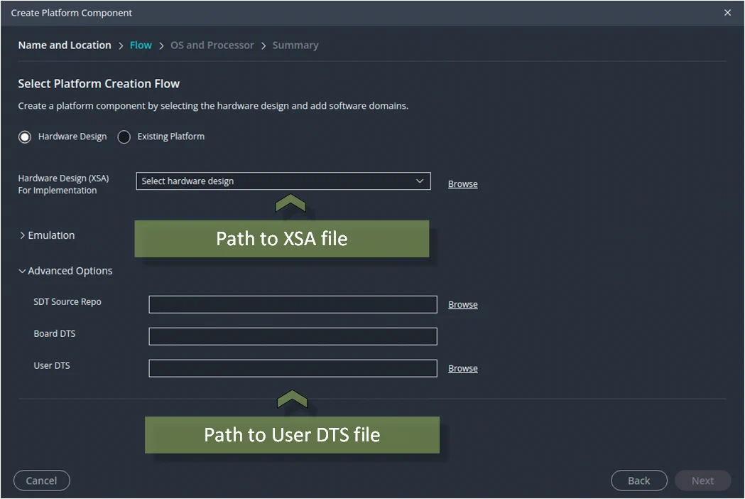
This means that when we begin developing the bare-metal application for the ZCU106, the build system already “knows” about the video pipeline running on the external FPGA (the Artix UltraScale+ of the AUBoard). When the AUBoard is connected to the ZCU106 via the SFP link, the complete system becomes operational. We can now develop and debug it as a single system from Vitis through a JTAG connection to the ZCU106 board.
In this article, I’ve discussed the challenges involved in creating a modular solution for connecting FPGAs to MIPI CSI-2 image sensors. We looked at a potential solution to this problem: designing an FMC with its own FPGA, and we discussed some of the advantages of this architecture.
We then explored how the new Vitis SDT flow provides a clean and maintainable way to deal with multi-FPGA architectures, providing us a path for simple integration of this FMC with a carrier board. Finally, I demonstrated our work to verify the design using off-the-shelf hardware with a prototype built from the AMD ZCU106 and the Tria AUBoard. For those who wish to reproduce our proof-of-concept, the source code can be downloaded from our Github: MIPI over Chip2Chip.
Some problems are best solved through multi-FPGA architectures. As FPGA designers, it’s important to recognize when this approach is appropriate and to understand the tools—such as the Vitis SDT flow—that can help us to work with these systems.