What am I learning here?
In this post we’ll look at using the Base System Builder in EDK version 13.1. Specifically you’ll learn:
- How to create an EDK project with the Base System Builder
- How to add a software application to an EDK project
- How to implement and test your design
Requirements
You will need the following :
- One ML505/ML506/ML507 or XUPV5 board (or actually any board supported by Xilinx).
- Xilinx ISE Design Suite 13.1 (including EDK)
Create the Basic Project
Follow these steps to create the basic project:
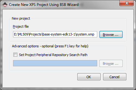
- Open XPS by selecting “Start->Xilinx ISE Design Suite 13.1->EDK->Xilinx Platform Studio”.
- From the dialog box, select “Base System Builder wizard” and OK.
- You will be asked to specify which folder to place the project. Click “Browse” and create a new folder for the project. Click “OK”.
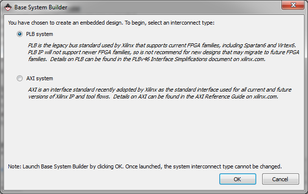
- The first page of the wizard will ask us to choose between using a Processor Local Bus (PLB) or an Advanced Extensible Interface (AXI). As we are using the Virtex-5, we have to select a PLB system, but if you are working with a Virtex-6 or a Spartan-6 you are better to go with the AXI system.
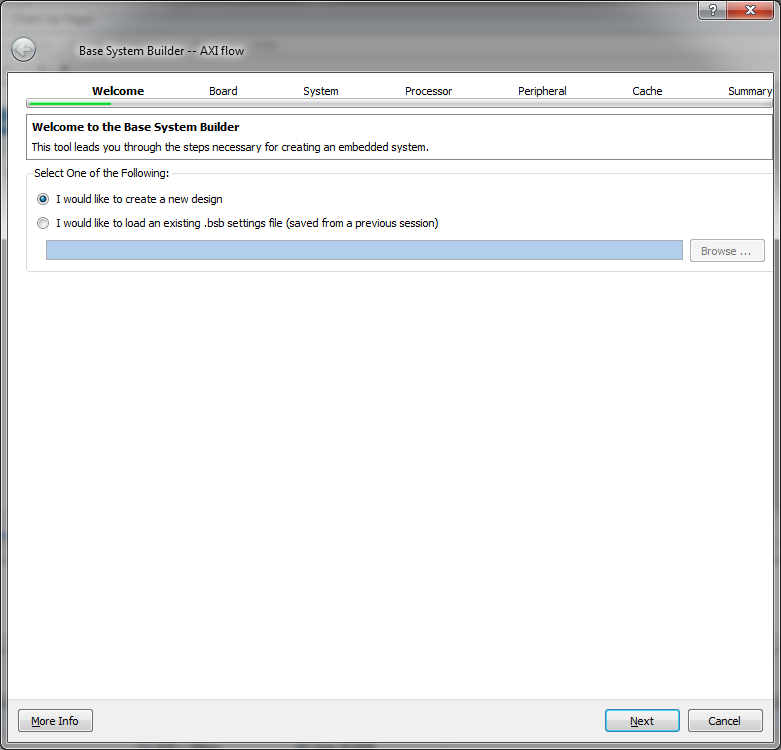
- We are given the choice to create a new project or to create one using the template of another project. Tick “I would like to create a new design” and click “Next”.
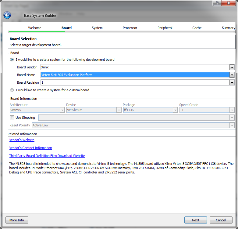
- On the “Select Board” page, select “Xilinx” as the board vendor. Then select the board you are using (eg. “Virtex 5 ML505 Evaluation Platform”). Select “1” as the board revision. Click “Next”. (Note: If you are using the XUPV5 (ML509) board, select “Virtex 5 ML505 Evaluation Platform” instead.)
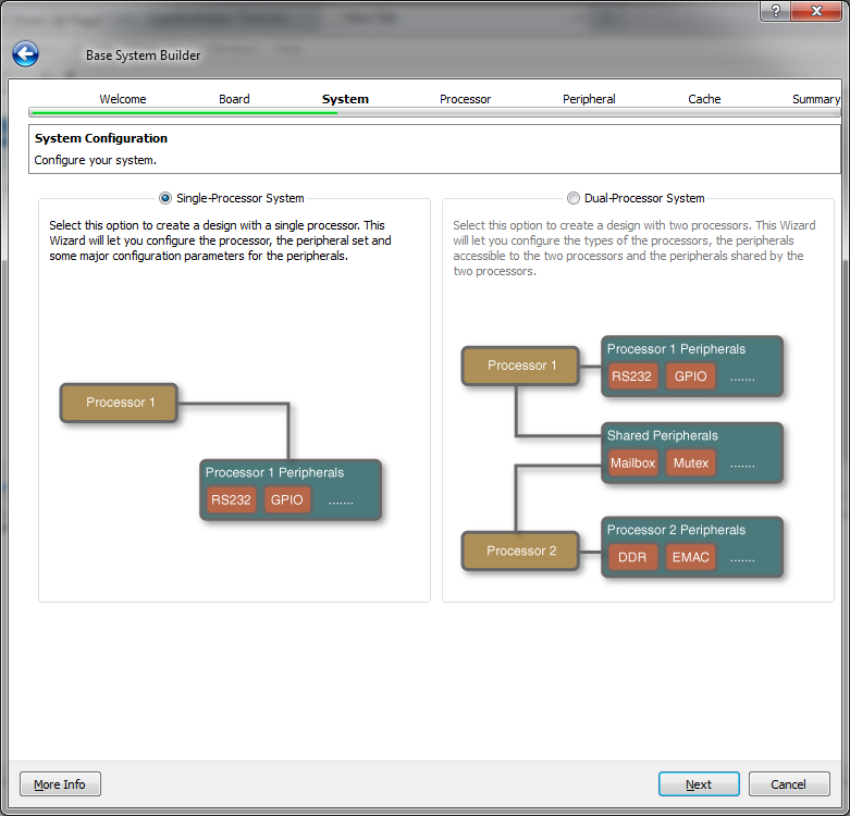
- Now we have the choice to build a single-processor or dual-processor system. The Virtex-5 doesn’t have any hard processors, so the Base System Builder will setup a Microblaze soft processor for us. Select “Single-Processor System” and click “Next”.
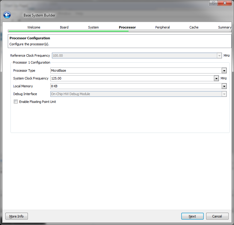
- On the “Configure Microblaze” page, we can specify the clock frequency of our processor and the amount of memory it will use. Select the clock frequency to 125MHz. Click “Next”.
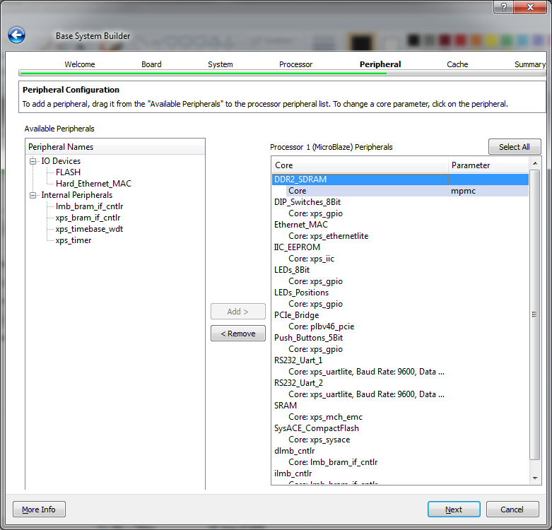
- Now we can select the peripherals to put in the design. The peripherals will all be connected to the Microblaze processor via the PLB and they allow us to control and access features of the FPGA and external hardware such as the DDR2 memory and the Ethernet MAC. We will leave the default setting which is to include ALL the standard peripherals. You might ask “Why include all the peripherals?”, well most of the time you would only include the peripherals that you need so that you don’t waste time building peripherals you wont use. In this case, I want you to include all the peripherals because a lot of the following EDK tutorials will be based on this “base system”. This way, we wont have to go through the Base System Builder for every tutorial and we’ll save time. The fact is, in a professional environment, you would never go through the Base System Builder when starting a new project, instead you would take an existing project and develop from that.
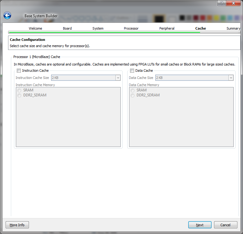
- In the next page we can configure cache memory for the Microblaze. In our case we wont use cache memory so leave the default and click “Next”.
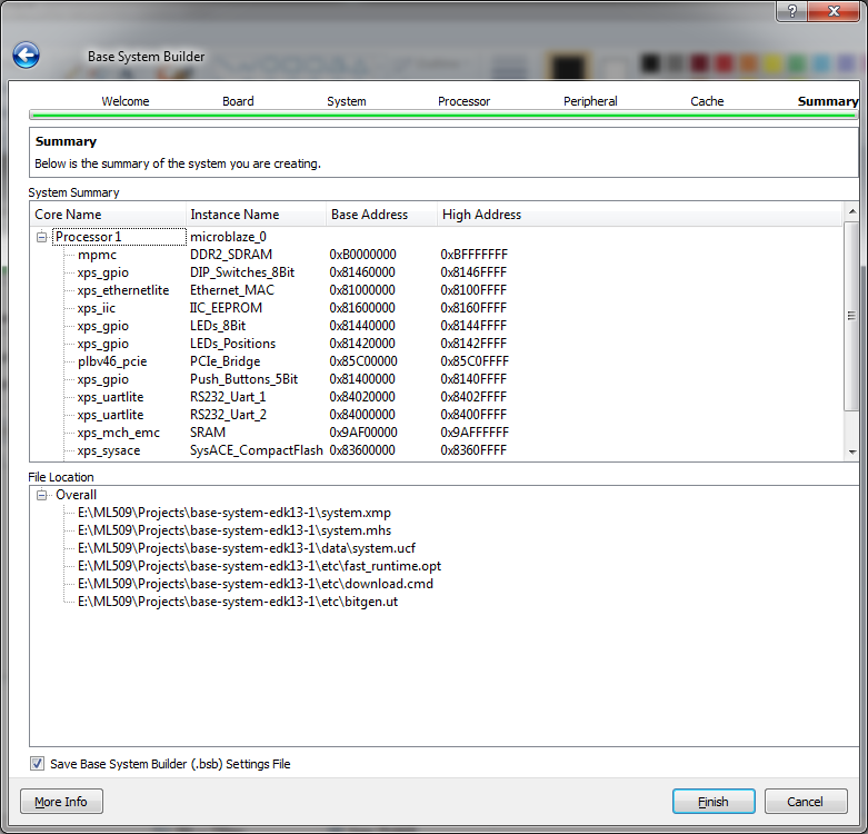
- The Base System Builder then gives us a summary of the design that it will create for us, showing the PLB memory map, the peripherals and the files that it will create.
- Click “Finish”.


If you are using the XUPV5 (ML509) board
If you are using the XUPV5 (ML509) board and you selected “Virtex 5 ML505 Evaluation Platform” in step 6 above, you will have to change the target FPGA setting to “XC5VLX110T”, package “FFG1136” and speed grade “-1” in the “Project->Project Options” menu. There are more changes to make that will be discussed in the next post: Convert an ML505 project for the XUPV5. If you don’t make these changes, you’ll find this error message when you try to build the bitstream:
ERROR:Place:713 - IOB component "fpga_0_DDR2_SDRAM_DDR2_DQ_pin<13>" and IODELAY
 component
 "DDR2_SDRAM/DDR2_SDRAM/mpmc_core_0/gen_v5_ddr2_phy.mpmc_phy_if_0/u_phy_io_0/g
 en_dq[13].u_iob_dq/u_idelay_dq" must be placed adjacent to each other into
 the same I/O tile in order to route net
 "DDR2_SDRAM/DDR2_SDRAM/mpmc_core_0/gen_v5_ddr2_phy.mpmc_phy_if_0/u_phy_io_0/g
 en_dq[13].u_iob_dq/dq_in". The following issue has been detected:
 Some of the logic associated with this structure is locked. This should cause
 the rest of the logic to be locked.A problem was found at site IODELAY_X0Y56
 where we must place IODELAY
 DDR2_SDRAM/DDR2_SDRAM/mpmc_core_0/gen_v5_ddr2_phy.mpmc_phy_if_0/u_phy_io_0/ge
 n_dq[13].u_iob_dq/u_idelay_dq in order to satisfy the relative placement
 requirements of this logic.  IODELAY
 DDR2_SDRAM/DDR2_SDRAM/mpmc_core_0/gen_v5_ddr2_phy.mpmc_phy_if_0/u_phy_io_0/ge
 n_dqs[0].u_iob_dqs/u_iodelay_dq_ce appears to already be placed there which
 makes this design unplaceable.
ERROR:Pack:1654 - The timing-driven placement phase encountered an error.
ERROR:Xflow - Program map returned error code 2. Aborting flow execution...
make: *** [__xps/system_routed] Error 1
Build the bitstream
The project is now ready to build.
- To build the bitstream of the project, select “Device Configuration->Update Bitstream”. This will take some time (around half an hour) depending on your machine.
You should end up seeing this message when the build is complete:
Checking platform address map ...

Initializing Memory...
Running Data2Mem with the following command:
data2mem -bm "implementation/system_bd" -p xc5vlx110tff1136-1 -bt
"implementation/system.bit"  -bd "bootloops/microblaze_0.elf" tag microblaze_0
-o b implementation/download.bit
Memory Initialization completed successfully.

Done!
What about the software application?
If you’re used to older versions of EDK, you would notice that we didn’t put any software into the project - software to run on the Microblaze processor. The reason for this is that Xilinx has removed this functionality from EDK in version 13.1. They gave us plenty of notice actually, but now all the software development for your FPGA projects must be done in SDK (Software Development Kit), logical isn’t it?
The project folder for this tutorial can be downloaded in a compressed ZIP file. Remember that if you want to understand the modifications made to the project for the XUPV5, you should read the next post.
Board
Virtex-5 Version
Project files
XC5VLX50T
XC5VSX50T
XC5VFX70T
XC5VLX110T