I just received the Zynq-7000 based ZC706 development board from a new client and I’m pretty excited to start working on it. This is the first time that I’ll be working on the Zynq FPGA, part of the latest series 7 devices from Xilinx, so over the next few days, I’ll be writing about my experiences while getting familiar with the board, the FPGA and version 14.5 of the Xilinx development tools. If I get time later, I might dive into the new Vivado Design Suite, promoted by Xilinx to be a “revolutionary IP-centric and system-centric design environment for dramatically faster integration and implementation” - we’ll see about that.
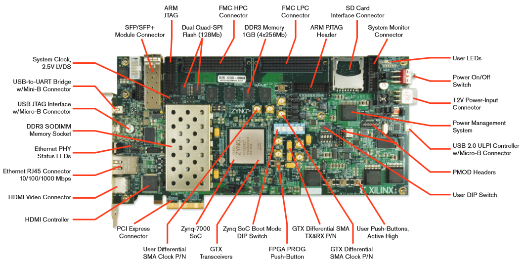
So what’s so great about this board? Apart from the Zynq-7000 with integrated ARM dual-core Cortex™-A9 processor (which I can’t wait to run Linux on), the board has all the high-speed interfaces you could want to get your data in and out. Here are the features according to the Xilinx website:
-
Zynq-7000 XC7Z045 FFG900 – 2
- ROHS compliant ZC706 kit including the XC7Z045 FFG900 – 2 SoC
-
Configuration
- Onboard configuration circuitry
- 2X16MB Quad SPI Flash
- SDIO Card Interface (boot)
- PC4 and 20 pin JTAG ports
-
Memory
- DDR3 Component Memory 1GB (PS)
- DDR3 SODIM Memory 1GB (PL)
- 2X16MB Quad SPI Flash (config)
- IIC - 1 KB EEPROM
-
Communication & Networking
- PCIe Gen2x4
- SFP+ and SMA Pairs
- GigE RGMII Ethernet (PS)
- USB OTG 1 (PS) - Host USB
- IIC Bus Headers/HUB (PS)
- 1 CAN with Wake on CAN (PS)
- USB UART (PS)
-
Video/ Display
- HDMI 8 color RGB 4.4.4 1080P-60 OUT
- HDMI IN 8 color RGB 4.4.4
-
Expansion Connectors
- 1st FMC LPC expansion port (LA LVDS Bus. 1 GT)
- 2nd FMC HPC expansion port (LA & HA LVDS Bus, 8 GT – No HB bus)
- Dual Pmod (8 I/O Shared with LED’s)
- Single Pmod (4 I/O)
- IIC access to 8 I/O
-
Clocking
- 33MHz PS System Clock
- 200MHz PL Oscillator (Single-Ended Differential)
- SMA Connectors for external clock (Differential)
- GTX Reference Clock port with 2 SMA connectors
- OBSAI/CPRI – SFP+ Received clock
- EXT Config CLK
-
Control & I/O
- 2 User Push Buttons/Dip Switch, 2 User LEDs
- IIC access to GPIO
- SDIO (SD Card slot)
- 3 User Push Buttons, 2 User Switches, 8 User LEDs
- IIC access to 8 I/O
- IIC access to a WTClock
-
Analog
- AMS interface (Analog) System Monitor and also available for external sensor
So over the next few days, I’ll need to get some basic designs working so that I can build upon them. For everything I get done, I’ll write a short tutorial so that others can also benefit from my experiences. Here are a few things I need to get going in the short term:
- Get a stand-alone program running on the ARM processor
- Get some basic communications between my PC and the ARM processor via the UART (UART over USB)
- Implement a VHDL peripheral and control it via the ARM processor - I’ll probably just get it to control the LEDs or something simple like that.
By the way, if you were wondering about the image at the top of the page, I made it using a scanner - it didn’t turn out the way I thought it would, but I like how the fan comes through sharp in front of a blurry background.