Xilinx just released a video presenting the next-generation of All Programmable devices and dev environments. It’s a quick look at where technology is going and particularly where FPGAs are going to make their mark.
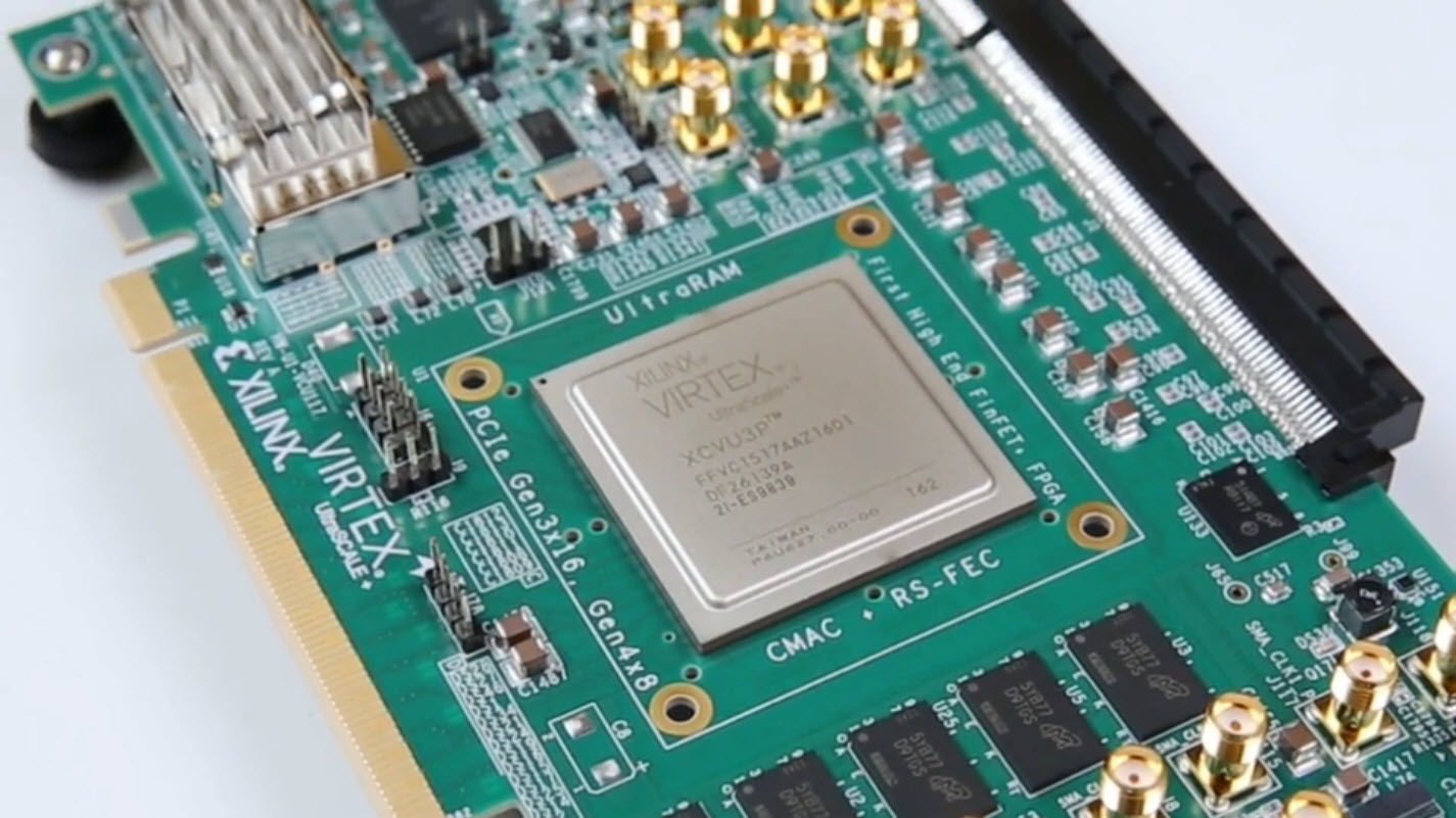
Of particular interest to me were the images of a Virtex Ultrascale PCI Express board at 2:45 in the video. This board appears to have both the PCIe gold-finger edge connector and a PCIe saddle-mount socket connector, so it could be used as either the PCIe end-point or the root complex - or maybe both at the same time. Most of Xilinx’s dev boards have the PCIe edge connector but as far as I know, the only FPGA dev board with a PCIe socket is the Mini-ITX from Avnet.
Although I don’t really know why you’d want to use both the edge connector and socket at the same time, I can come up with a few crazy ideas:
- Stack-up multiple FPGA accelerators (although physically you wouldn’t be able to fit too many of these into a server)
- Connect a PCIe NVMe SSD to the socket and use the FPGA to offload data processing operations such as hash function for database applications (although the better way to do it would be to have the FPGA interface directly with NAND flash)
- Use the FPGA as a bridge between a root-complex and end-point, and to perform analysis of PCIe transactions with the aim of identifying inefficiencies, bottle-necks or opportunities for hardware acceleration in a particular system.
If you’ve got any other ideas for potential applications for this board, feel free to leave a comment below.