Title here
Summary here
Tutorial on creating a Microblaze-based PCIe Root Complex design in Vivado to connect an NVMe SSD.
April 13, 201618 minutes
This is the first part of a three part tutorial series in which we will go through the steps to create a PCI Express Root Complex design in Vivado, with the goal of being able to connect a PCIe end-point to our FPGA. We will test the design on hardware by connecting a PCIe NVMe solid-state drive to our FPGA using the FPGA Drive adapter.
Part 1: Microblaze PCI Express Root Complex design in Vivado (this tutorial)
In the first part of this tutorial series we will build a Microblaze based design targeting the KC705 Evaluation Board. In the second part, we will build a Zynq based design targeting the PicoZed 7Z030 and PicoZed FMC Carrier Card V2. In part 3, we will test the design on the target hardware using a stand-alone application that will validate the state of the PCIe link and perform enumeration of the PCIe end-points. We will then run PetaLinux on the FPGA and prepare our SSD for use under the operating system.
To complete this tutorial you will need the following:
Note: The tutorial text and screenshots are suitable for Vivado 2015.4 however the sources in the Git repository will be regularly updated to the latest version of Vivado.
The image below gives us a high level view of the design showing each component and how it connects to the Microblaze - only the AXI-Lite interfaces are shown.
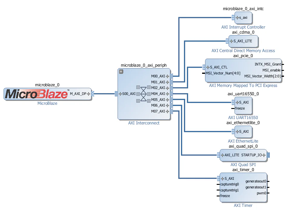
Let’s talk about the role of each peripheral in the design:
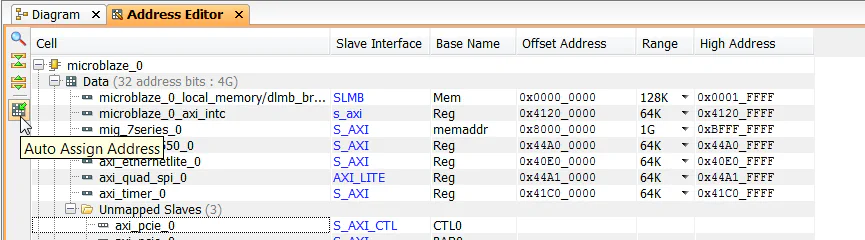
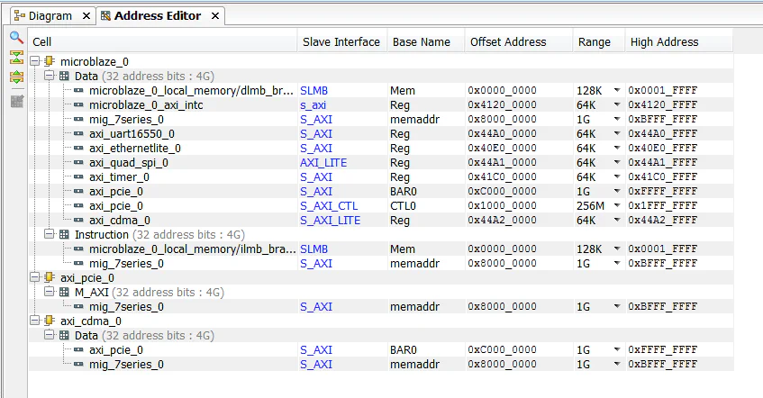
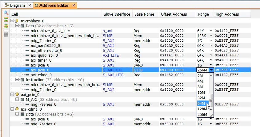
The image below shows the AXI memory mapped interface connections which is useful for understanding the memory spaces and the devices that have access to them.
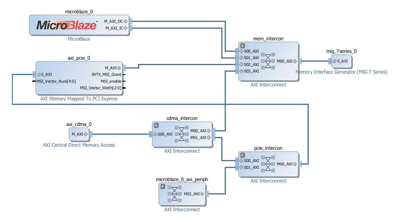
The important thing is to understand is who the bus masters are and what address spaces they can access - the connections could have been made in a number of different ways to achieve the same goal.
The 2 address spaces are:
The 3 AXI masters and the address spaces they can access are:
About PCIe end-point bus mastering
Most PCIe end-points have bus mastering capability. Basically this means that the PCIe end-point can send memory read/write TLPs to the root complex and read/write to a part of the system memory that was allocated for the end-point. Maybe the most common application of end-point bus mastering is the implementation of Message Signaled Interrupts (or MSI). When a PCIe end-point generates an MSI, it simply writes to part of the system memory that was allocated by the root complex.
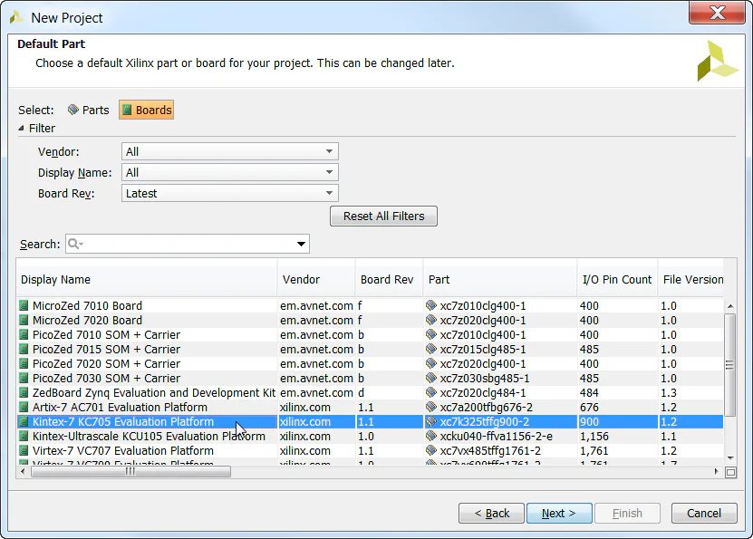
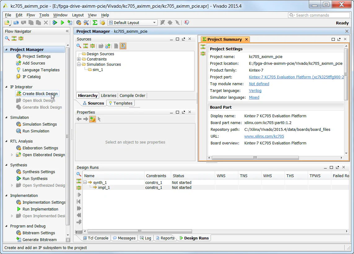
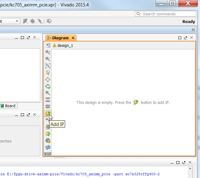
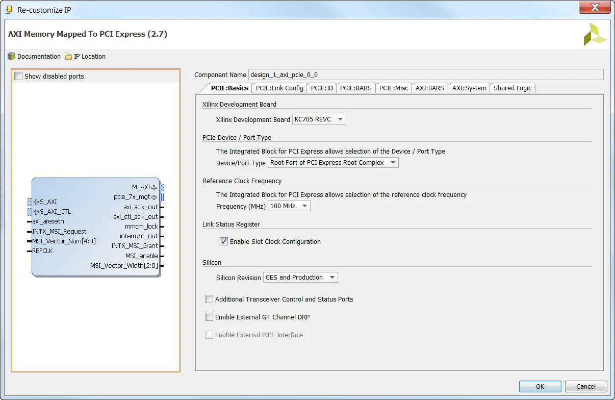
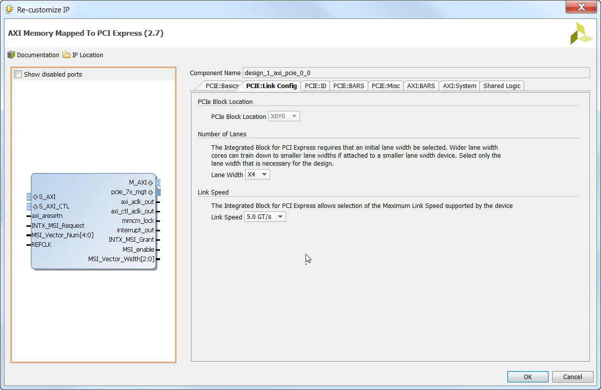
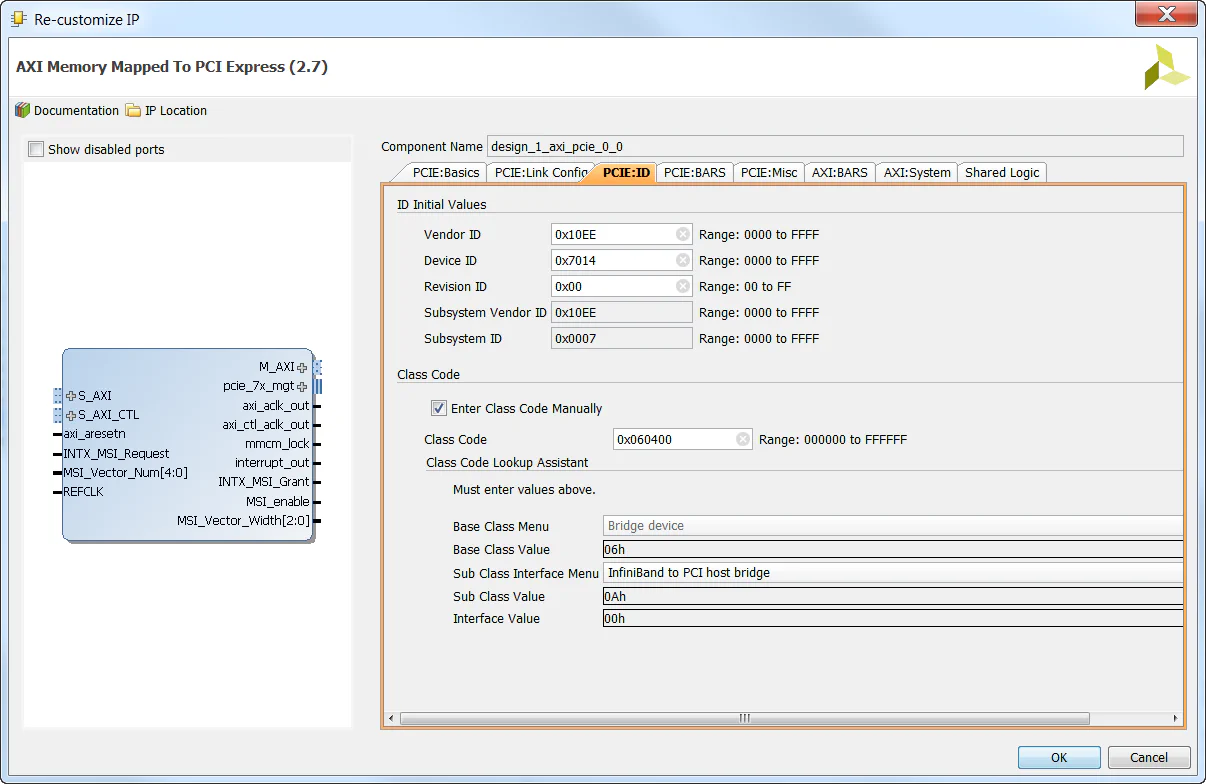
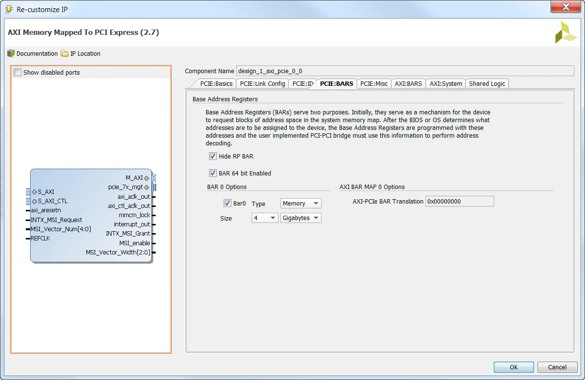
We start by creating a new project in Vivado and selecting the KC705 Evaluation board as our target.
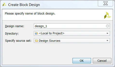
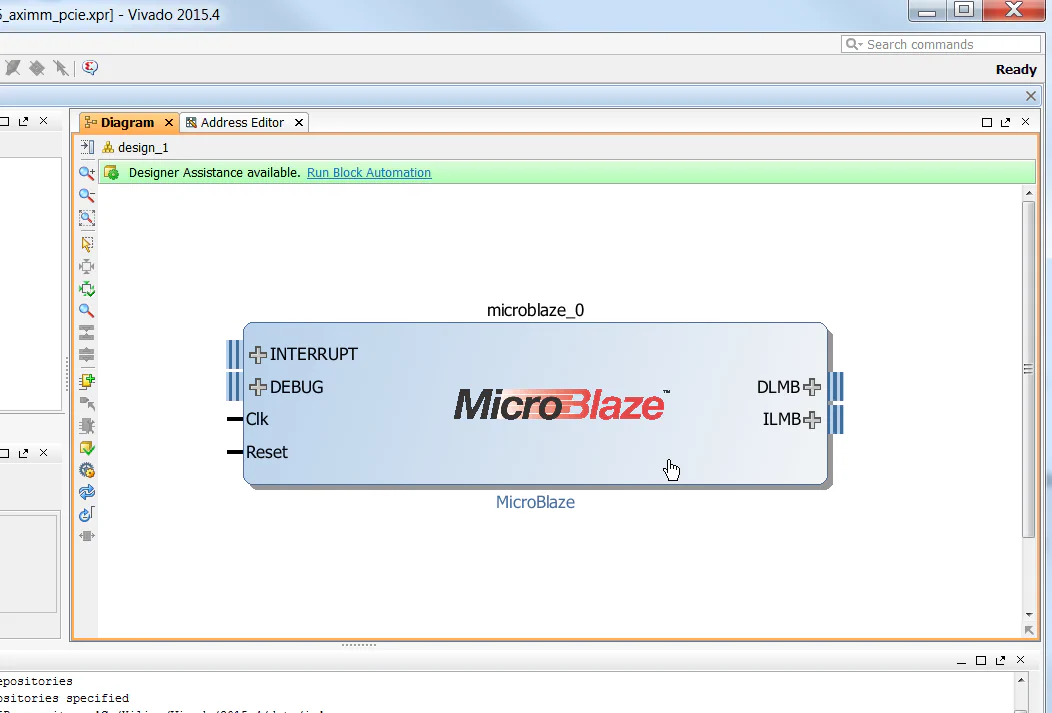
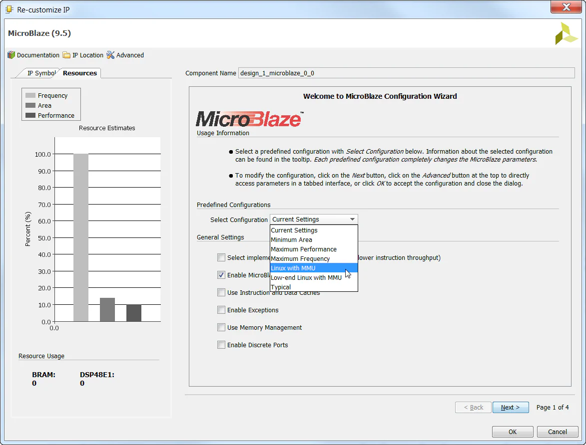
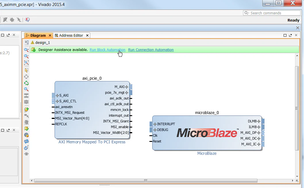
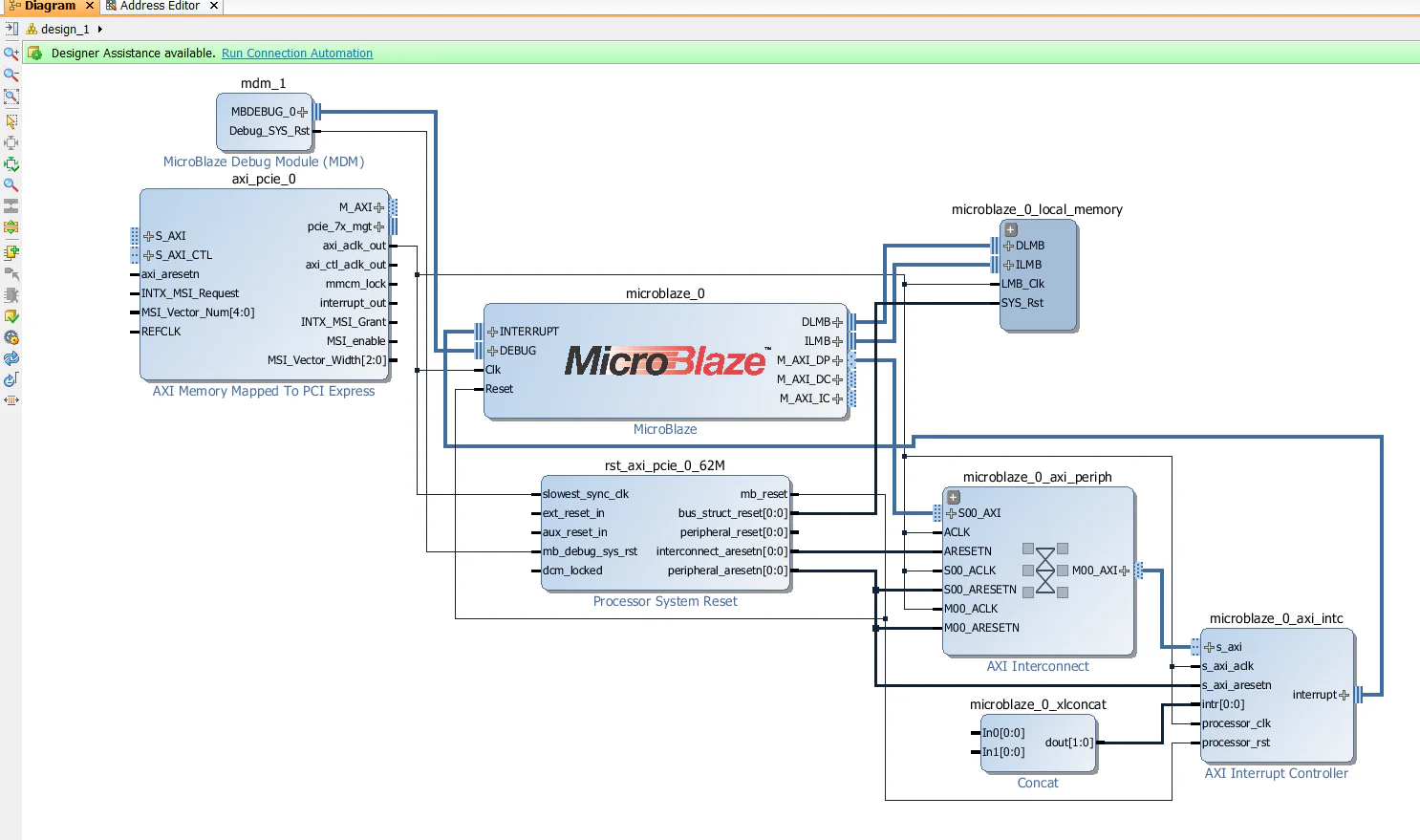
Now we need to create and build our block design. We will start by adding the Microblaze and the AXI Memory Mapped PCI Express Bridge.
/axi_pcie_0/axi_aclk_out. Then click OK.
axi_aclk_out clock which is driven by the AXI-PCIe block. The reset signals are generated by the Processor System Reset block, which will synchronize the external reset pushbutton signal to the axi_aclk_out clock.
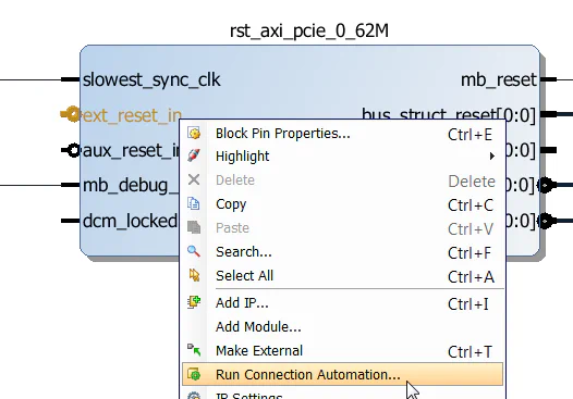
ext_reset_in input of the rst_axi_pcie_0_62M Processor System Reset and select “Run Connection Automation”, then click OK. This will connect the reset input to the KC705’s reset pushbutton.
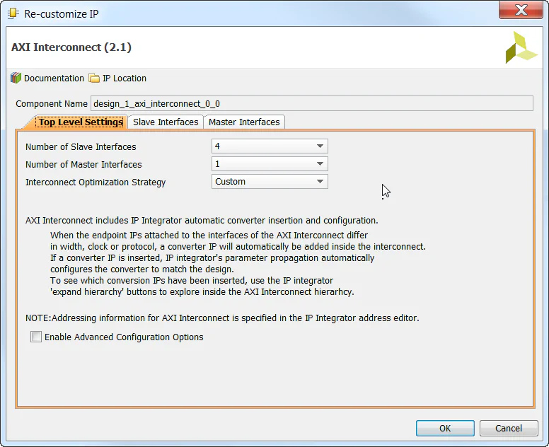
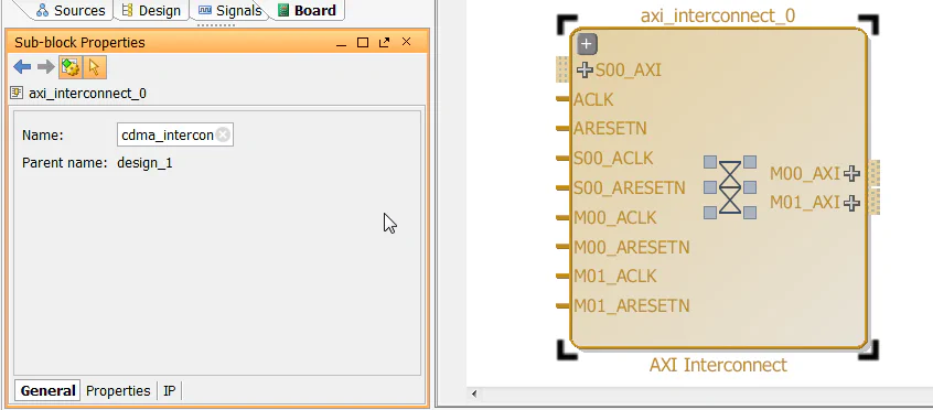
mem_intercon using the “Sub-block properties” window.
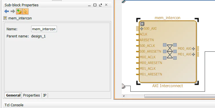
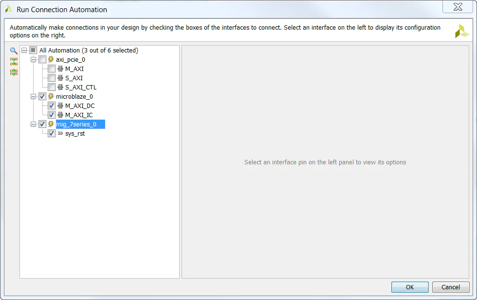
mem_intercon block and configure it for 4 slave interfaces, and 1 master interface.
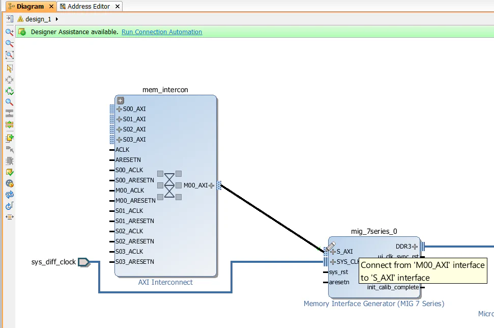
mem_intercon to the slave interface (S_AXI) of the MIG.
microblaze_0/M_AXI_DC, microblaze_0/M_AXI_IC and mig_7series_0/sys_rst connections. Click “OK”.
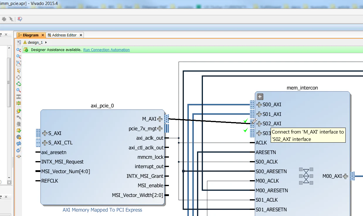
axi_pcie_0 to the slave interface (S02_AXI) of the mem_intercon. This provides a data path from the PCIe end-point to the DDR3 memory. Note that the PCIe end-point will not be able to access anything else in our design.
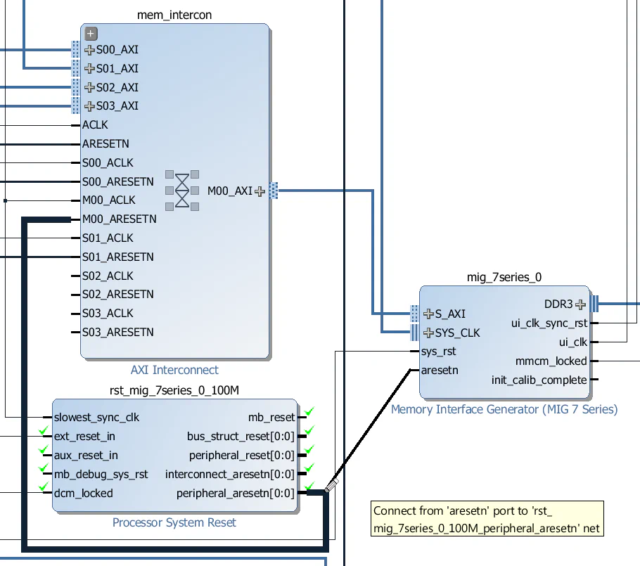
peripheral_aresetn output of the rst_mig_7series_0_100M Processor System Reset block. Note that this Processor System Reset was generated when we used the connection automation feature in the steps above.
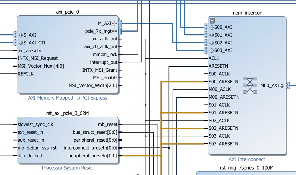
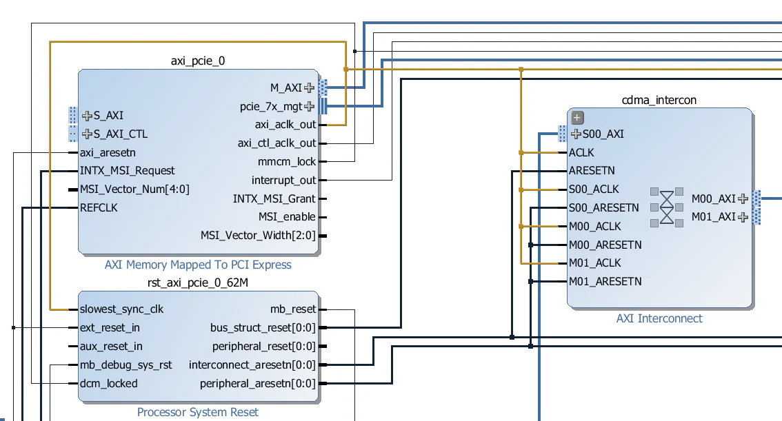
S02_ACLK and S03_ACLK clock inputs of the mem_intercon to the axi_aclk_out output of the AXI-PCIe block. Also connect the S02_ARESETN and S03_ARESETN inputs to the peripheral_aresetn of the rst_axi_pcie_0_62M Processor System Reset.
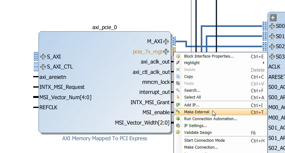
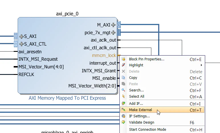
pcie_7x_mgt port of the AXI-PCIe block and select “Make External”. This will connect the gigabit transceivers to the 4 PCIe lanes on the PCIe edge-connector of the
KC705.
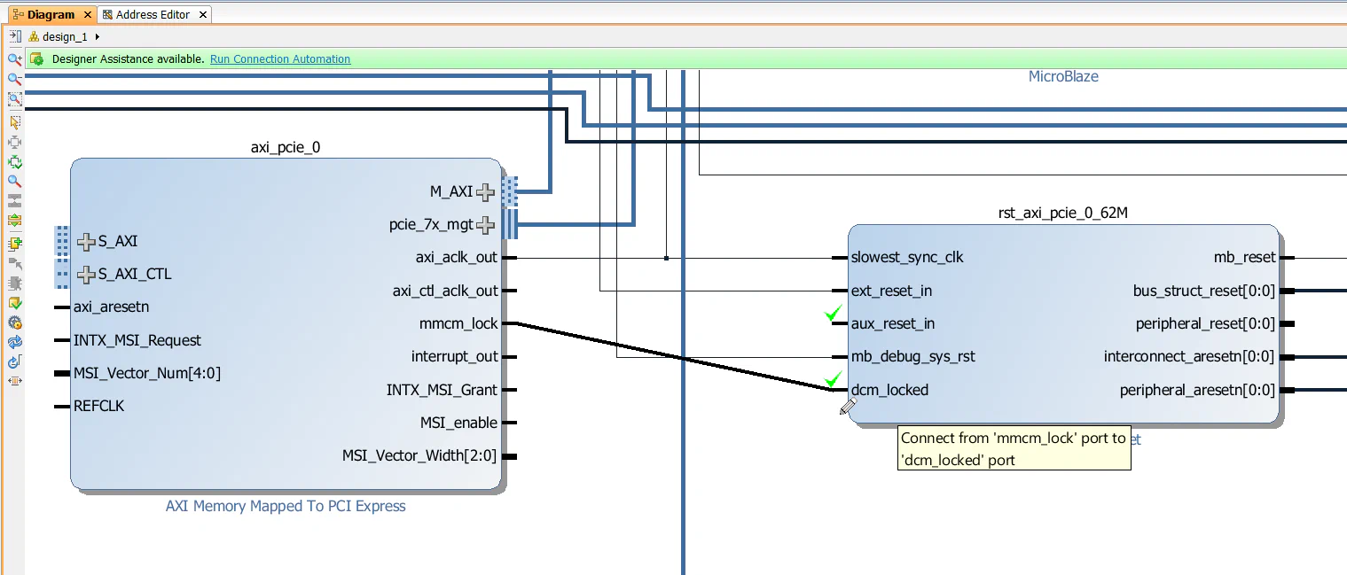
mmcm_lock output of the AXI-PCIe block to the dcm_locked input of rst_axi_pcie_0_62M Processor System Reset block.
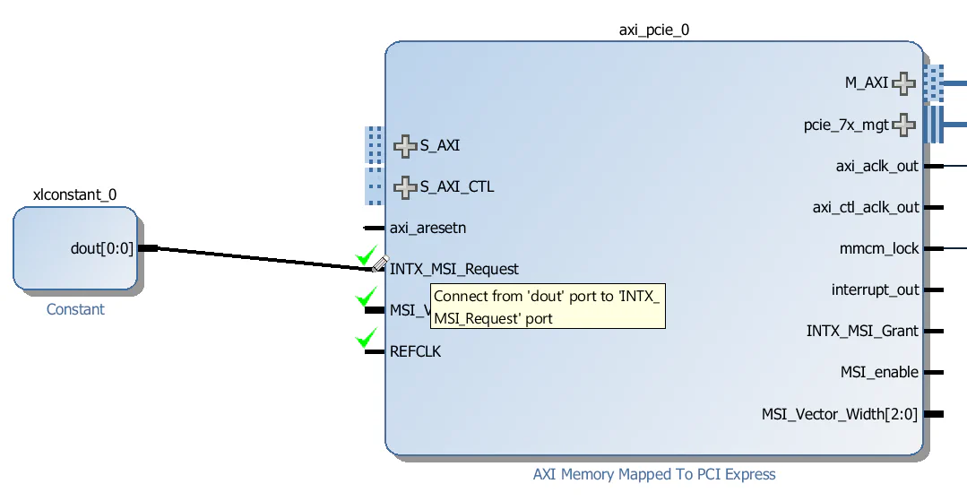
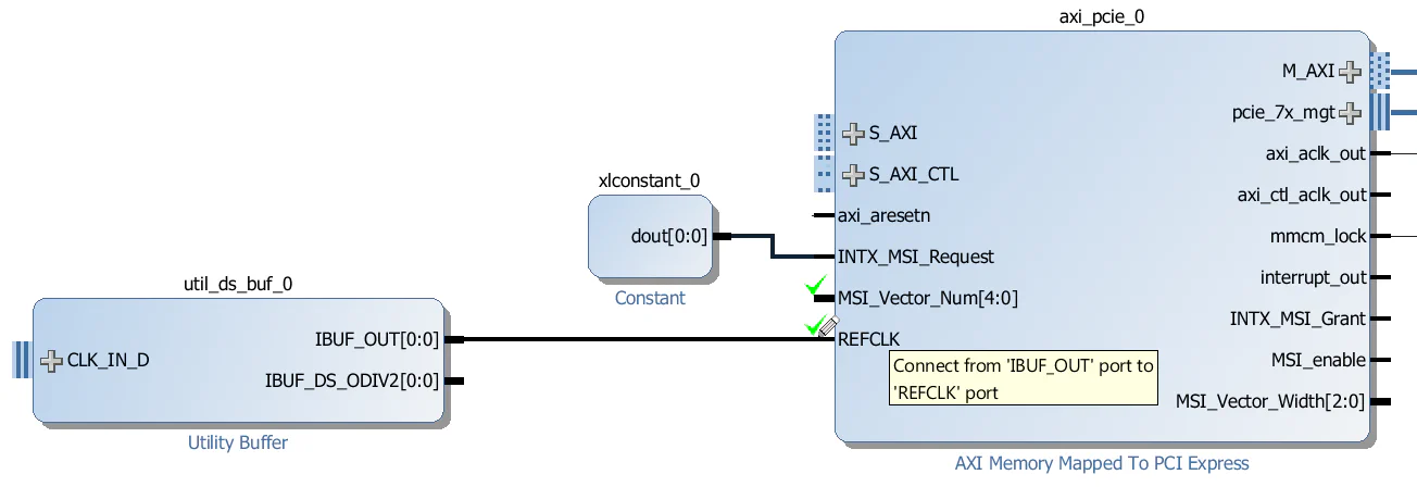
INTX_MSI_Request input of the AXI-PCIe block. Connect the constant’s output to the INTX_MSI_Request input of the AXI-PCIe block.
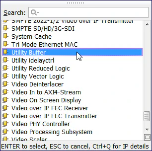
IBUF_OUT output of the utility buffer to the “REFCLK” input of the AXI-PCIe block.
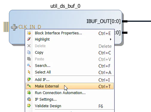
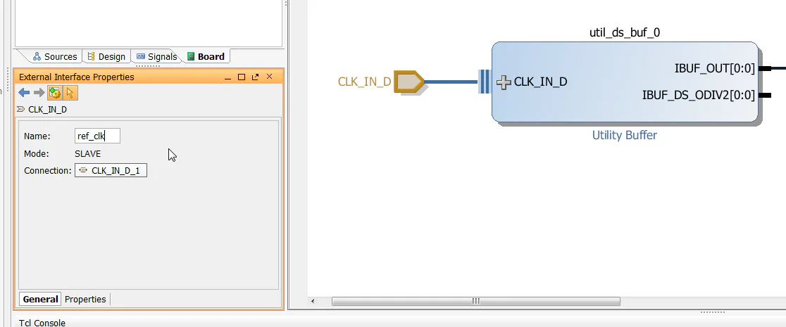
CLK_IN_D input of the utility buffer and select “Make External”.
ref_clk using the External Interface Properties window.
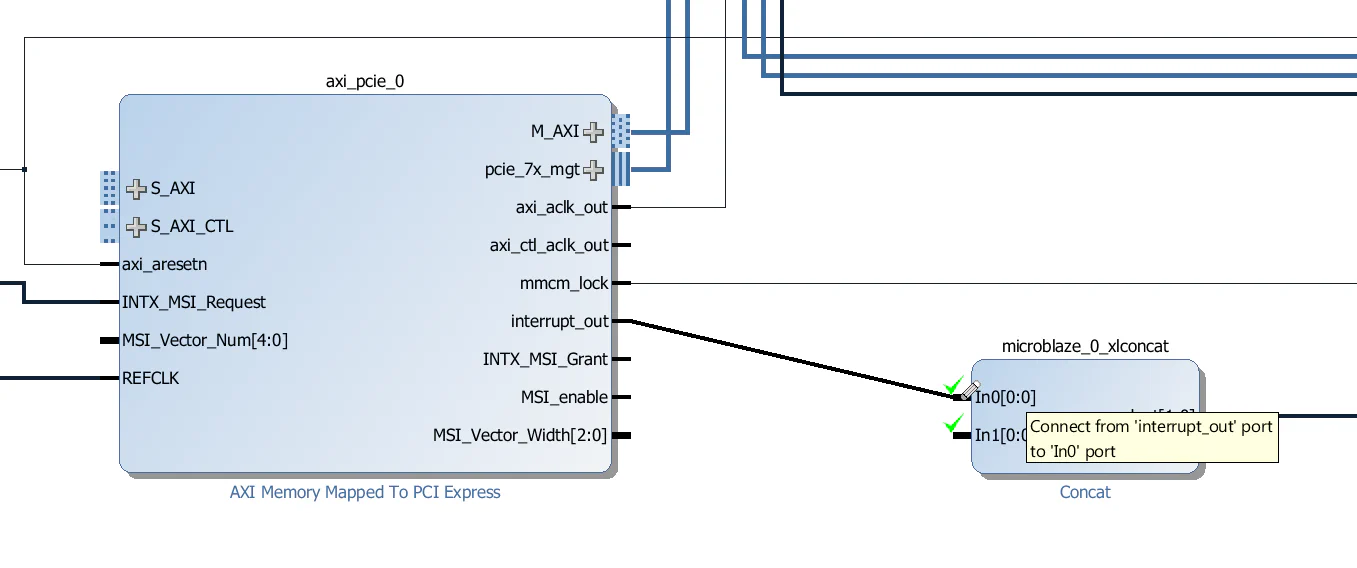
interrupt_out output of the AXI-PCIe block to the “In0” input of the interrupt concat microblaze_0_xlconcat.
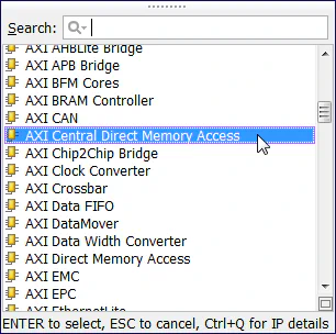
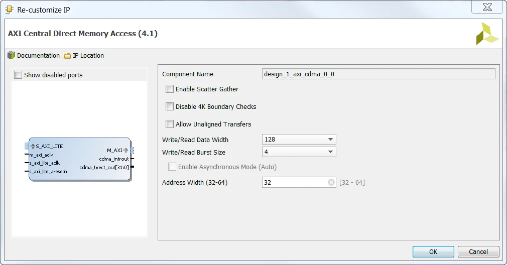
Now we’ll add a Central DMA to this design which will allow us to setup data transfers between the PCIe end-point and the DDR3 memory. We won’t actually test the CDMA in this tutorial series, but it’s an important part of any PCIe design that needs to transfer large amounts of data very quickly over the PCIe link. We will add an AXI Interconnect to allow the CDMA to access both the PCIe end-point and the MIG.
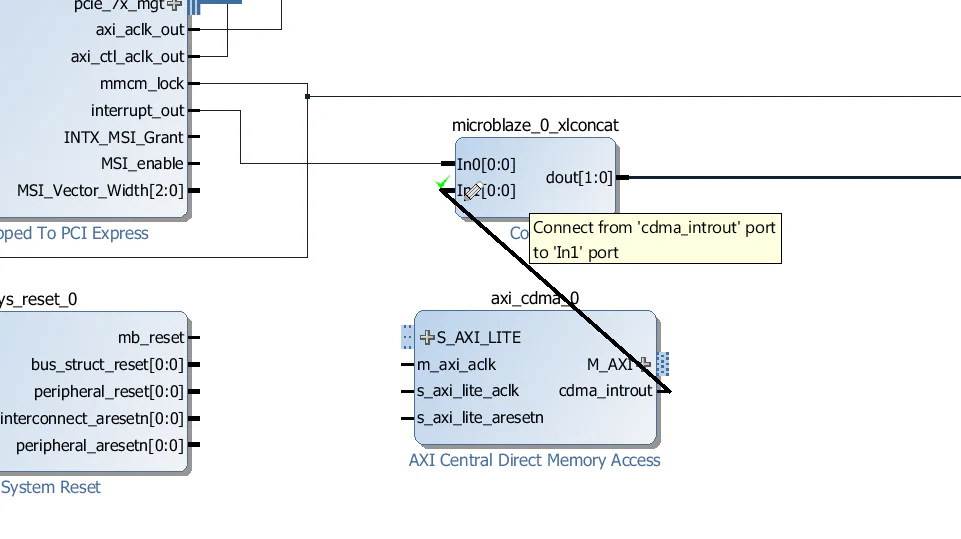
cdma_introut output of the CDMA to the “In1” input of the interrupt concat microblaze_0_xlconcat.
cdma_intercon using the “Sub-block Properties” window.
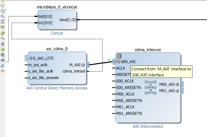
M_AXI interface of the CDMA to the S00_AXI interface of the cdma_intercon.
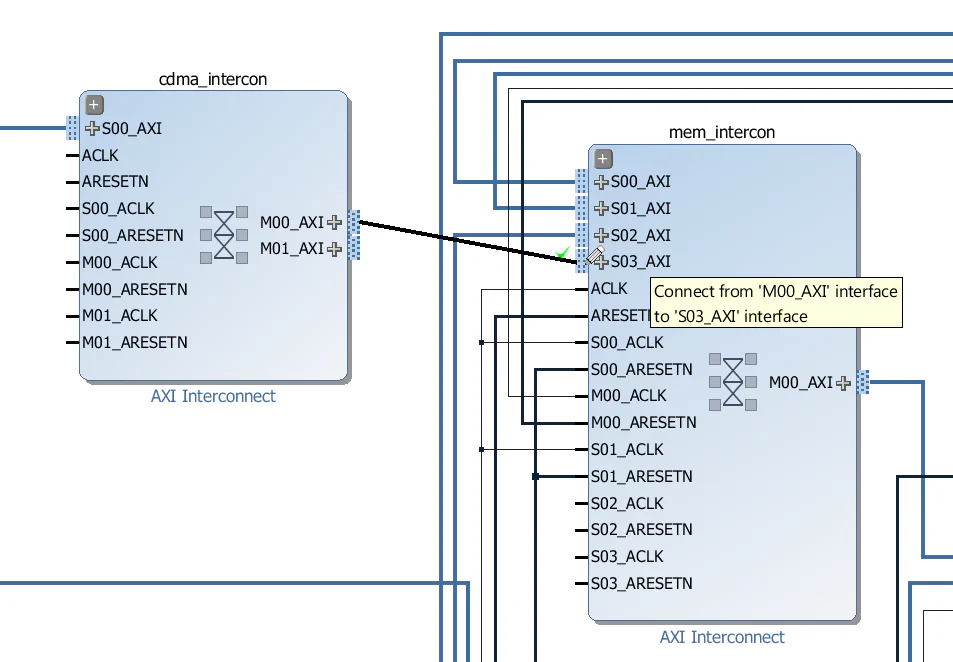
M00_AXI interface of the cdma_intercon to the S03_AXI interface of the mem_intercon. This provides the data path between the CDMA and the DDR3 memory.
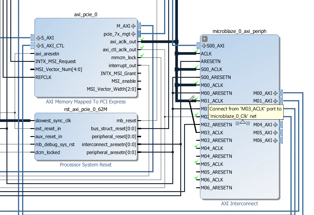
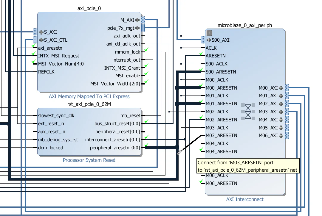
cdma_intercon as shown in the image below. Connect all the clock inputs to the axi_aclk_out output of the AXI-PCIe block. Connect the “ARESETN” input to the interconnect_aresetn output of the rst_axi_pcie_0_62M Processor System Reset. Connect all other reset inputs to the peripheral_aresetn output of the rst_axi_pcie_0_62M Processor System Reset.
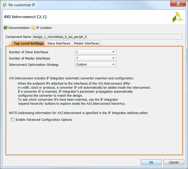
microblaze_0_axi_periph interconnect and configure it for 7 master ports. Leave the number of slave ports as 1.
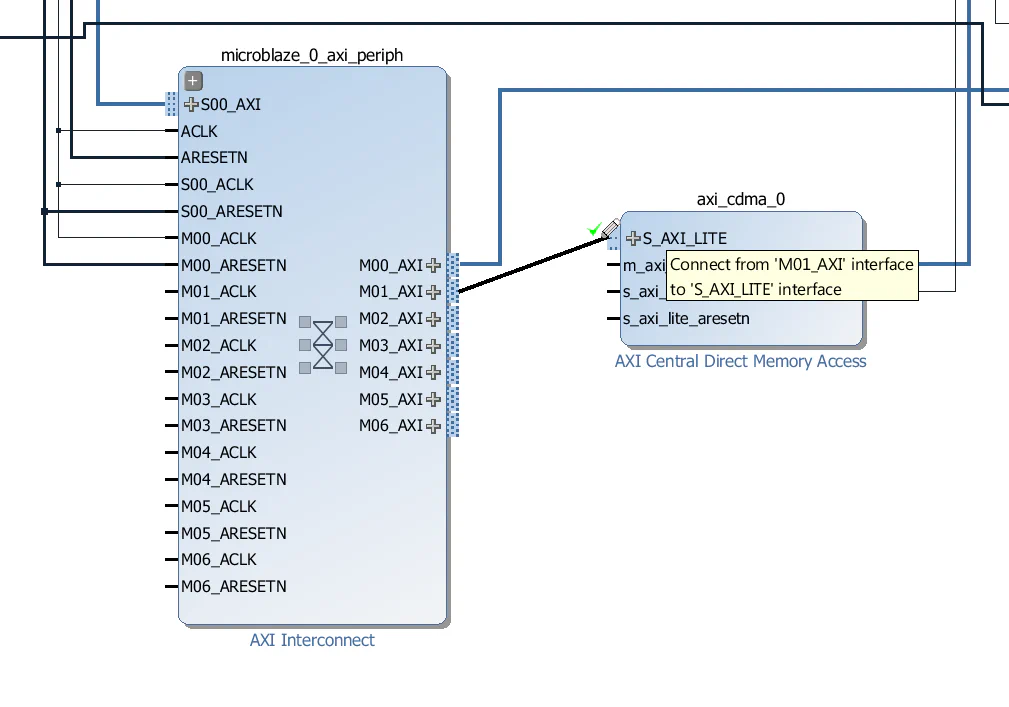
M01_AXI interface of the microblaze_0_axi_periph interconnect to the S_AXI_LITE interface of the CDMA.
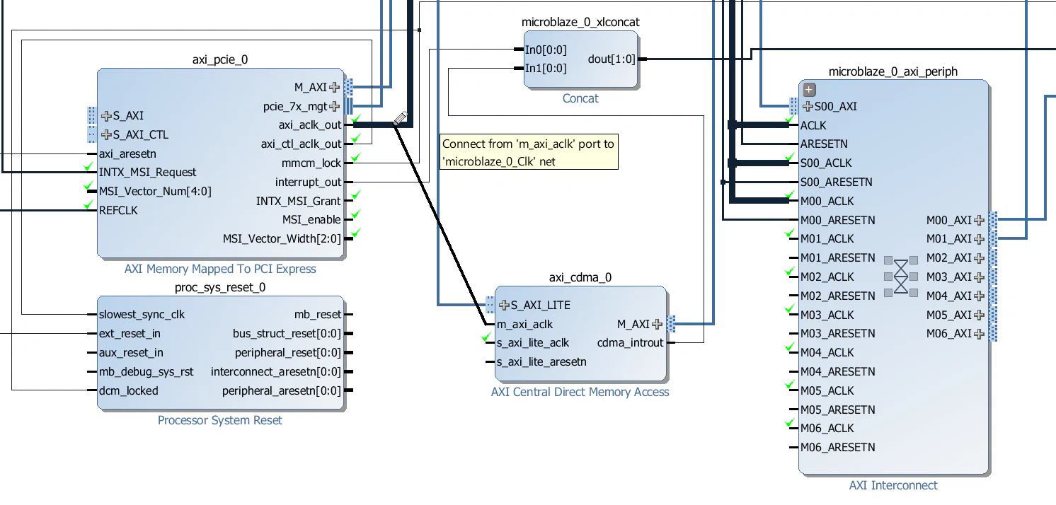
m_axi_aclk input of the CDMA to the axi_aclk_out output of the AXI-PCIe block.
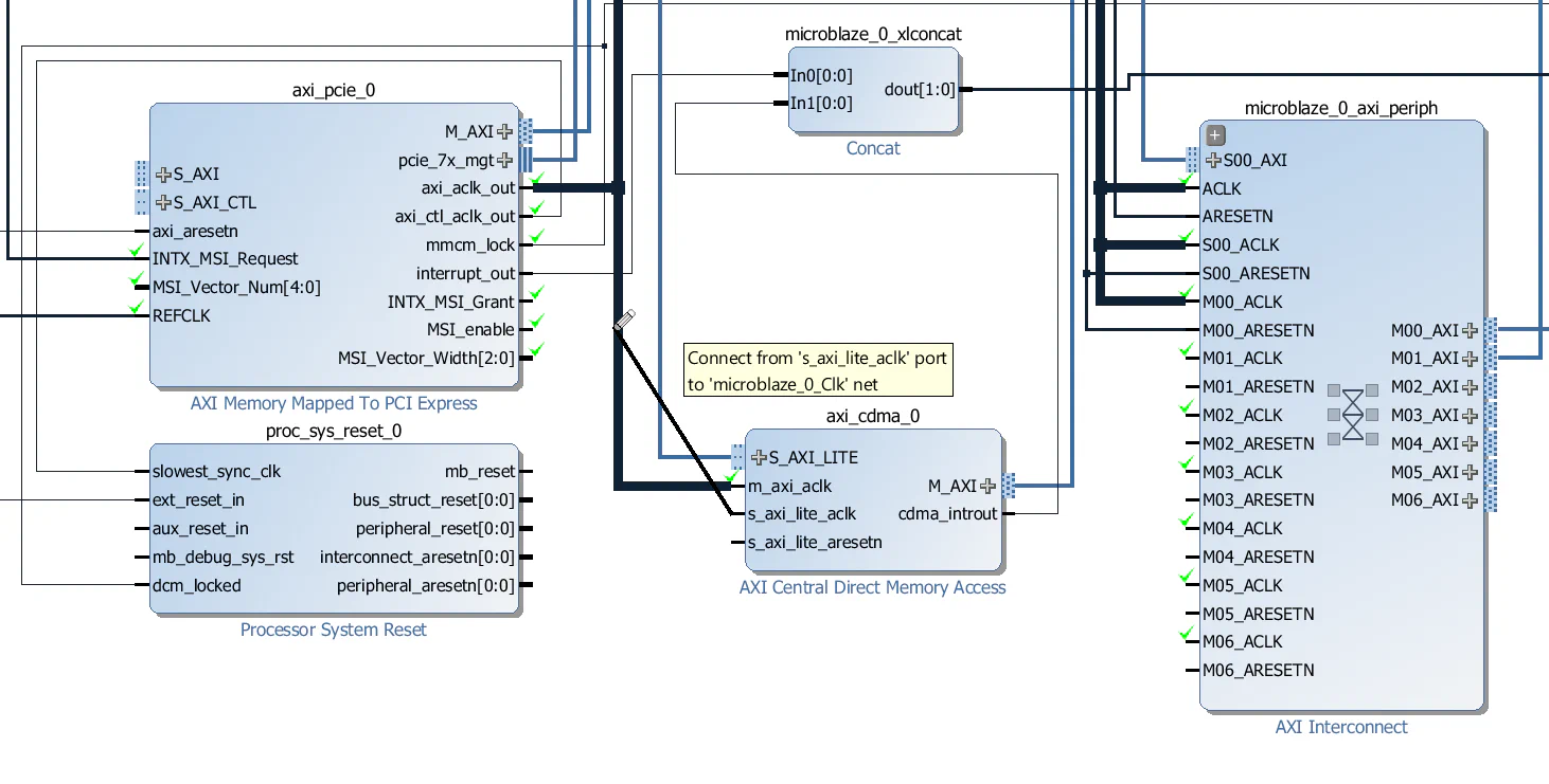
s_axi_lite_aclk input of the CDMA to the axi_aclk_out output of the AXI-PCIe block.
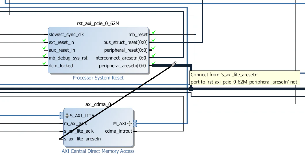
s_axi_lite_aresetn input of the CDMA to the peripheral_aresetn output of the rst_axi_pcie_0_62M Processor System Reset block.
M01_ACLK input of the microblaze_0_axi_periph to the axi_aclk_out output of the AXI-PCIe block.
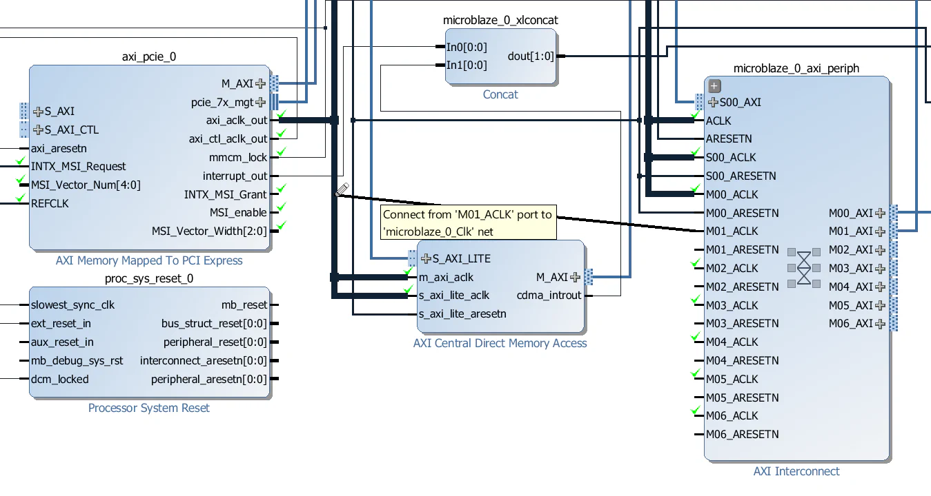
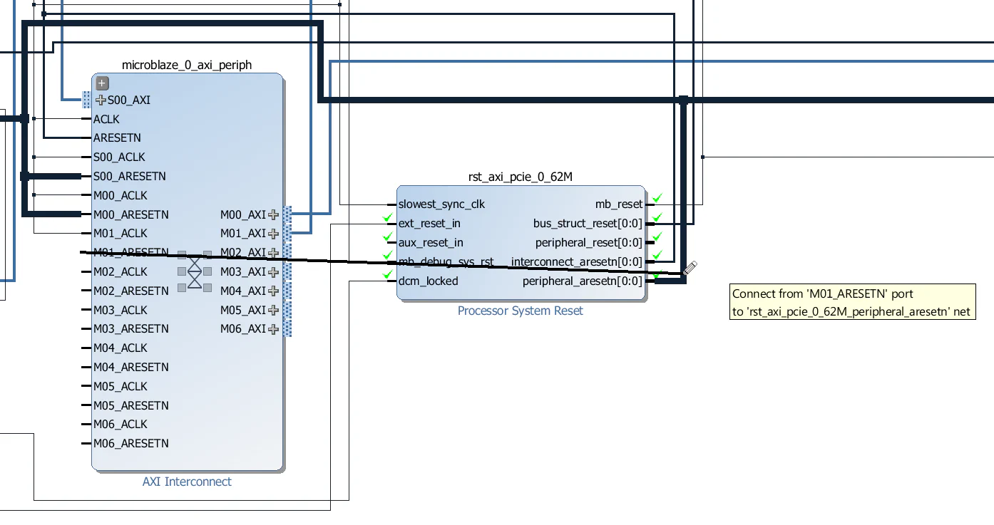
M01_ARESETN input of the microblaze_0_axi_periph to the peripheral_aresetn output of the rst_axi_pcie_0_62M Processor System Reset block.
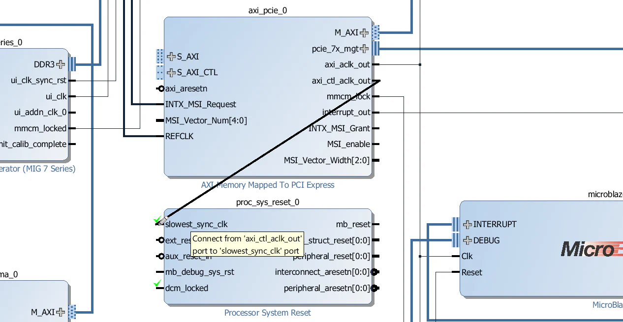
The AXI PCIe block has one slave interface for configuration (S_AXI_CTL) and another for accessing the PCIe end-point (S_AXI). The slave interface for configuration must be driven synchronous to the axi_ctl_aclk_out clock, so before connecting the slave interfaces, we first need to create a Processor System Reset to generate a reset signal that is synchronous to this clock.
axi_ctl_aclk_out clock output of the AXI-PCIe block to the slowest_sync_clk input of the Processor System Reset just added.
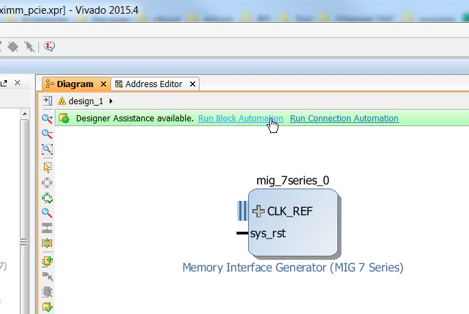
ext_reset_in input of the Processor System Reset and select “Run Connection Automation”, then click OK.
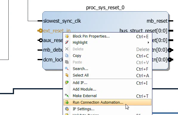
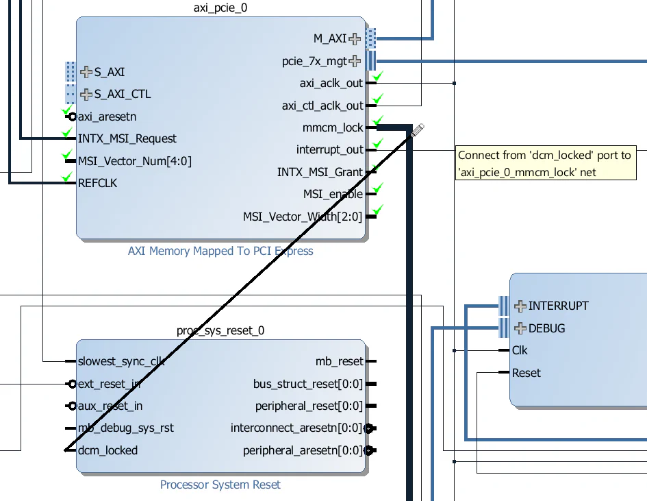
dcm_locked input of the Processor System Reset to the mmcm_lock output of the AXI-PCIe block.
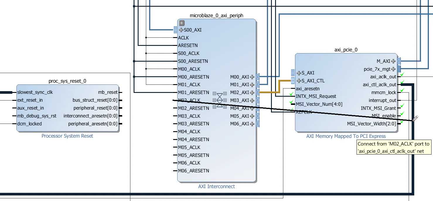
M02_AXI interface of the microblaze_0_axi_periph interconnect to the S_AXI_CTL interface of the AXI-PCIe block.
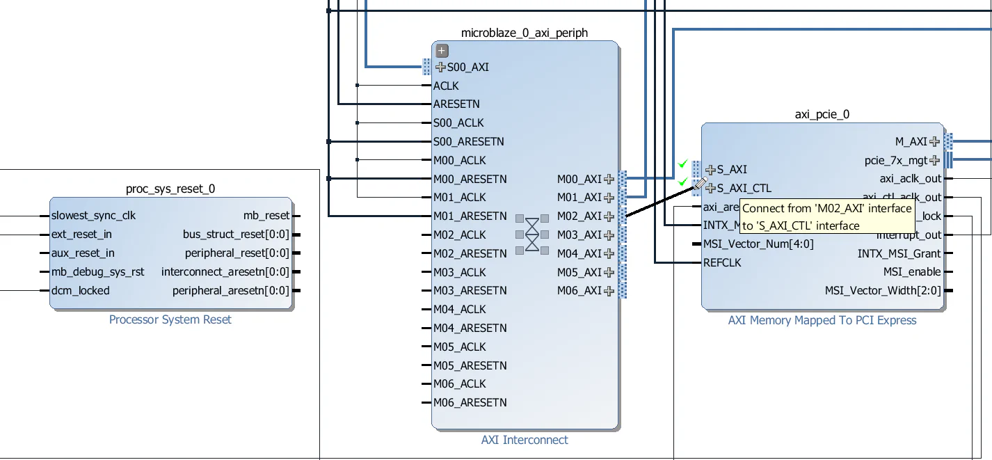
M02_ACLK input of the microblaze_0_axi_periph interconnect to the axi_ctl_aclk_out output of the AXI-PCIe block.
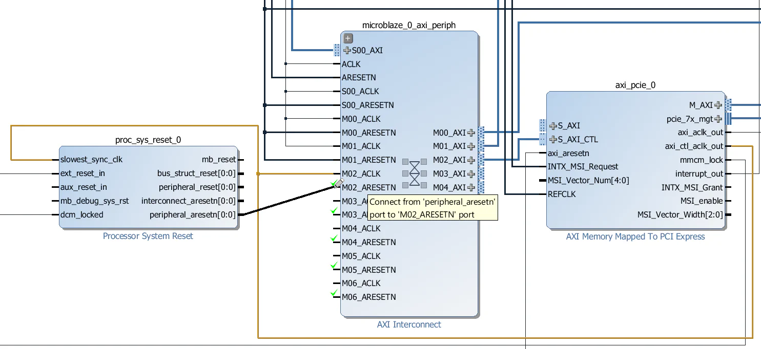
peripheral_aresetn output of the proc_sys_reset_0 Processor System Reset to the M02_ARESETN input of the microblaze_0_axi_periph interconnect.
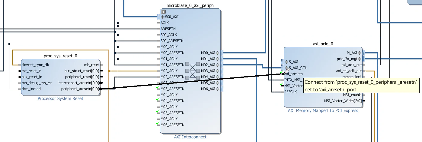
peripheral_aresetn output of the proc_sys_reset_0 Processor System Reset to the axi_aresetn input of the axi_pcie_0 block.
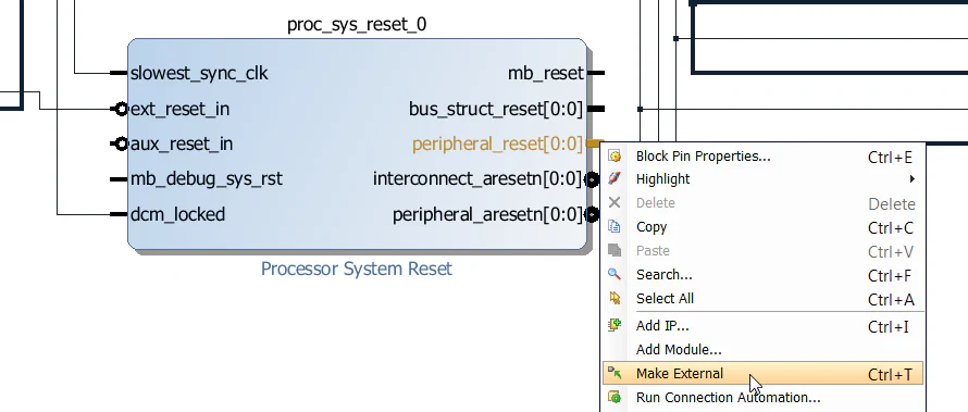
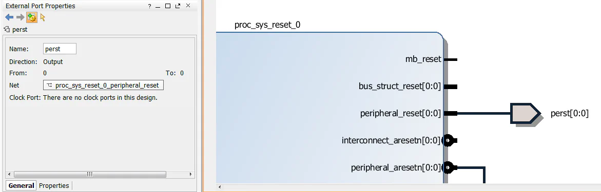
peripheral_reset output of the proc_sys_reset_0 Processor System Reset and click “Make External”.
The other slave interface of the AXI-PCIe block, S_AXI, provides access to the PCIe end-point address space. We want this port to be accessible to both the Microblaze and the CDMA, so we will add another AXI Interconnect to the design.
pcie_intercon and configure it to have 2 slave interfaces and 1 master interface.
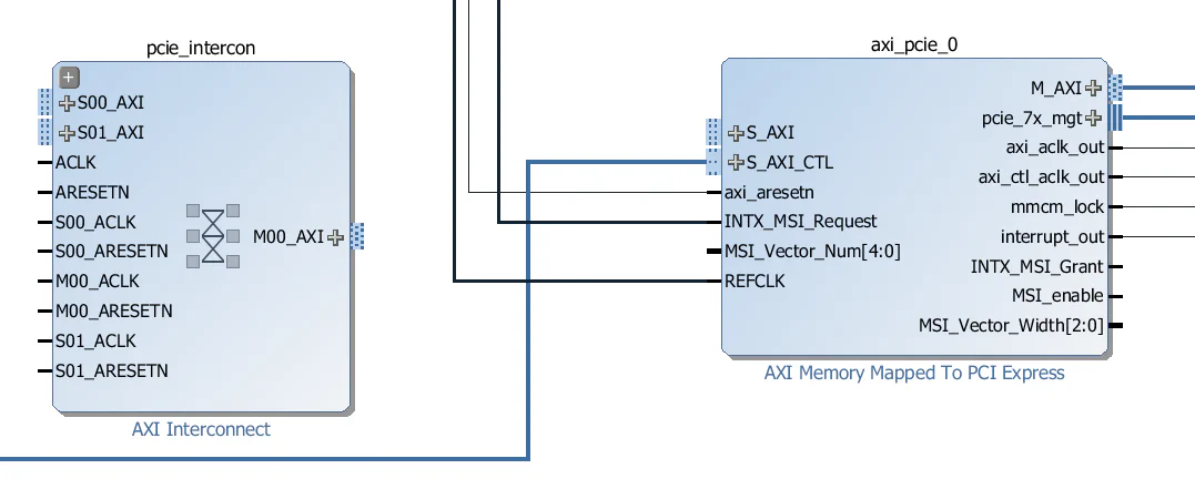
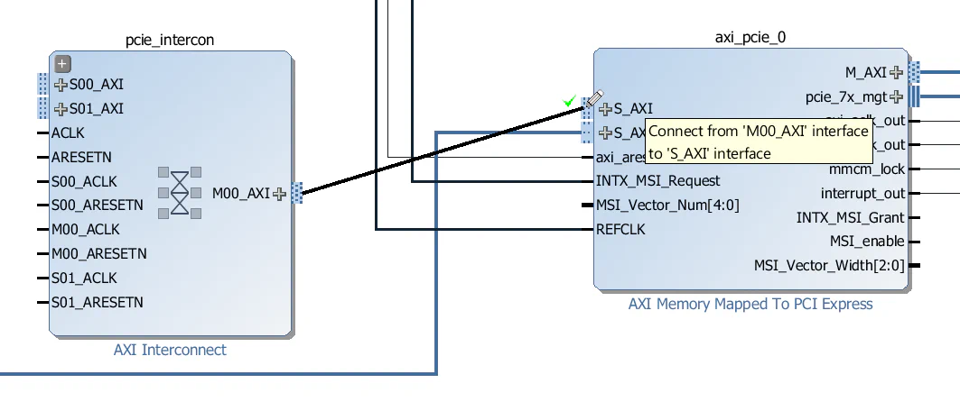
M00_AXI interface of the pcie_intercon to the S_AXI interface of the AXI-PCIe block.
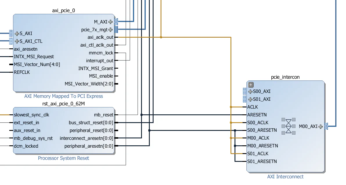
pcie_intercon as shown in the image below. Connect all the clock inputs to the axi_aclk_out output of the PCIe block. Connect the “ARESETN” input to the interconnect_aresetn output of the rst_axi_pcie_0_62M Processor System Reset. Connect all other reset inputs to the peripheral_aresetn output of the rst_axi_pcie_0_62M Processor System Reset.
M01_AXI interface of the cdma_intercon to the S00_AXI interface of the pcie_intercon.
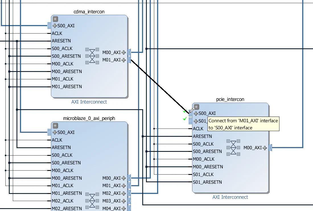
M03_AXI interface of the microblaze_0_axi_periph interconnect to the S01_AXI interface of the pcie_intercon.
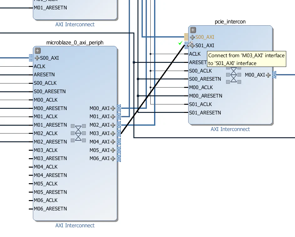
M03_ACLK input of the microblaze_0_axi_periph interconnect to the axi_aclk_out output of the AXI-PCIe block.
M03_ARESETN of the microblaze_0_axi_periph interconnect to the peripheral_aresetn of the rst_axi_pcie_0_62M Processor System Reset block.
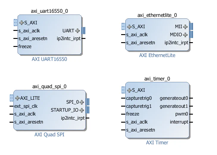
To make our design “Linux ready”, we need to add four more blocks to our design:
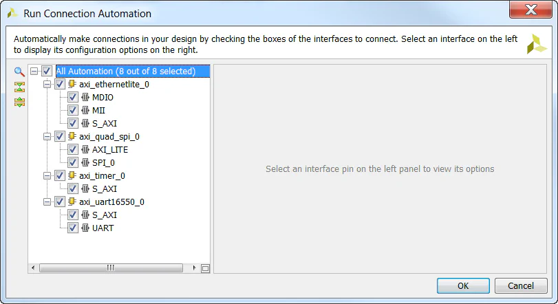
We will add all 4 blocks to the design and then let the block automation feature handle the connection of these peripherals to the Microblaze.
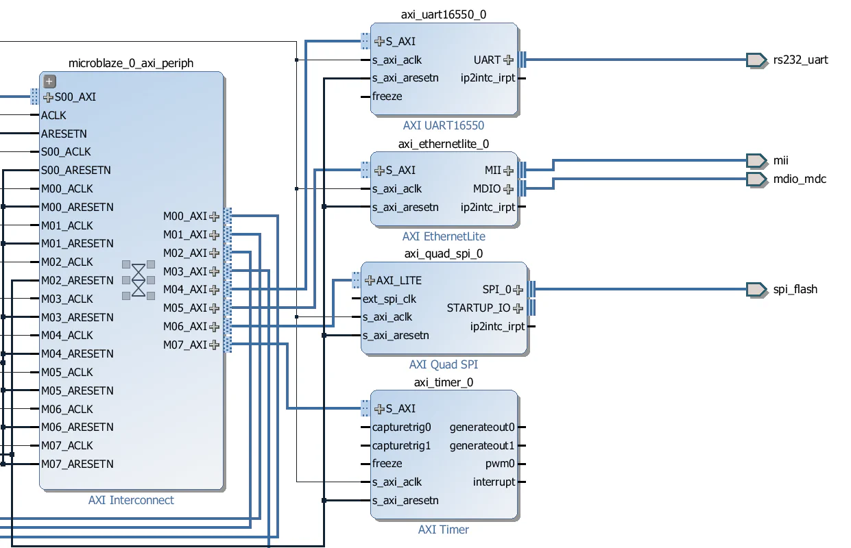
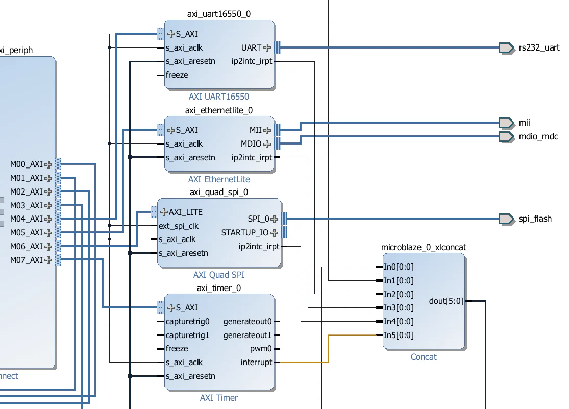
microblaze_0_axi_periph interconnect as shown in the image below.
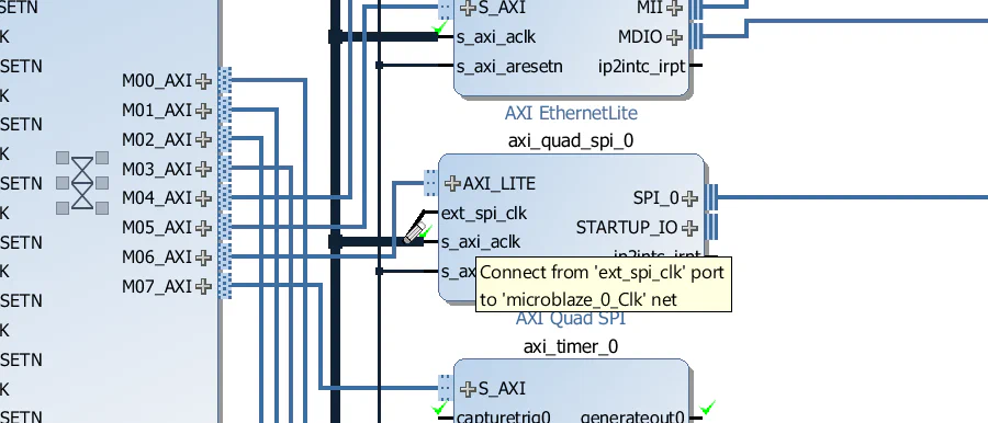
ext_spi_clk input of the AXI QSPI to the same clock as it’s s_axi_aclk input.
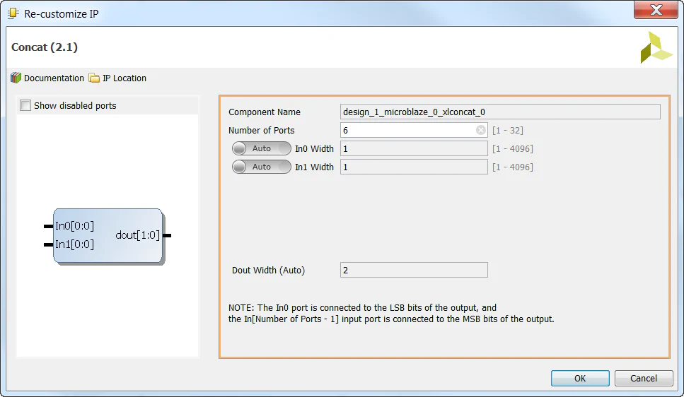
microblaze_0_xlconcat interrupt concat and change the number of input ports to 6 - we need 4 more to connect the interrupts of our new peripherals.
ip2intc_irpt. The interrupt output for the AXI Timer is called “interrupt”.
It’s always nice to have an LED light up to tell us that things are working correctly.
mmcm_lock output of the AXI-PCIe block and select “Make External”.
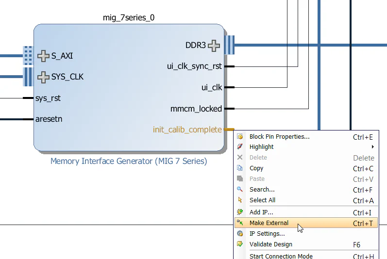
init_calib_complete output of the MIG and select “Make External”.
We will later add a constraint for each one of these ports to assign it to a specific LED on the KC705 board.
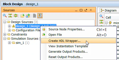
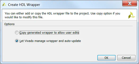
Now the block diagram is complete, so we can save it and create a HDL wrapper for it.
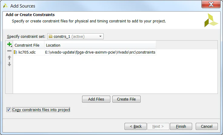
We must now add our constraints to the design for assignment of the PCIe integrated block, the gigabit transceivers, the reference clocks, the LEDs and a few other signals.
Finished at last!
In the next part of this tutorial series, we will build another PCIe Root Complex design in Vivado, but this time for the Zynq. The target hardware will be the PicoZed 7Z030 and the PicoZed FMC Carrier Card V2.
In the third and final part of this tutorial series, we will run a stand-alone application on the hardware which will check the state of the PCIe link and enumerate the connected PCIe end-points. Then we will run PetaLinux on our hardware and make an NVMe PCIe SSD accessible under the operating system.
The sources for re-generating this project automatically can be found on Github here: FPGA Drive PCIe Root Complex design
Here are some other useful resources for creating PCI Express designs:
If you have any questions about this tutorial, or if you run into problems, please leave me a comment below.