Title here
Summary here
Tutorial on creating a Zynq-based PCIe Root Complex design in Vivado to connect an NVMe SSD.
April 14, 201613 minutes
This is the second part of a three part tutorial series in which we will create a PCI Express Root Complex design in Vivado with the goal of connecting a PCIe NVMe solid-state drive to our FPGA.
Part 1: Microblaze PCI Express Root Complex design in Vivado
Part 2: Zynq PCI Express Root Complex design in Vivado (this tutorial)
In this second part of the tutorial series, we will build a Zynq based design targeting the PicoZed 7Z030 and PicoZed FMC Carrier Card V2. In part 3, we will then test the design on the target hardware by running a stand-alone application which will validate the state of the PCIe link and perform enumeration of the PCIe end-points. We will then run PetaLinux on the FPGA and prepare our SSD for use under the operating system.
To complete this tutorial you will need the following:
Note: The tutorial text and screenshots are suitable for Vivado 2015.4 however the sources in the Git repository will be regularly updated to the latest version of Vivado.
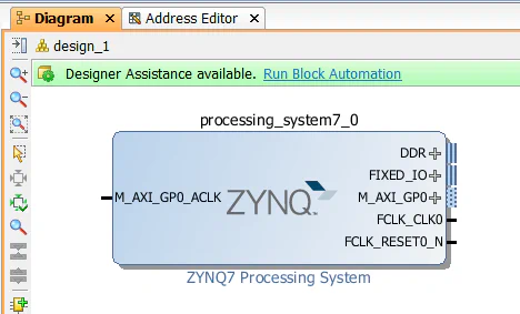
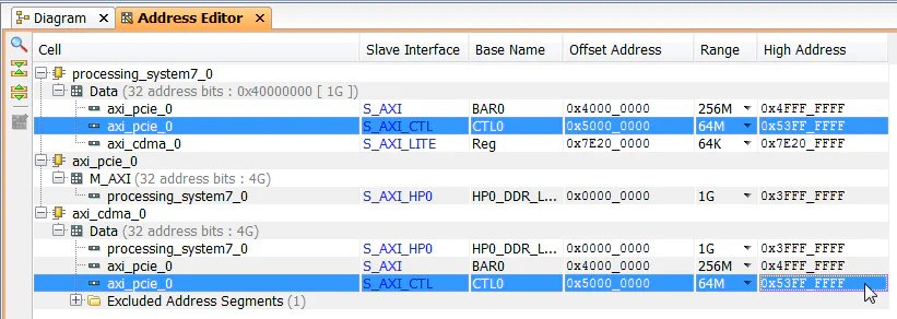
The diagram below shows the block design we are about to build with only the AXI interfaces showing. It shows three main elements: the Zynq PS, the AXI to PCIe bridge and the AXI CDMA. If you went through the previous tutorial where we created the same design for a Microblaze system, you may be wondering why the Zynq design seems so much simpler. The reason is that a lot of the elements required in this design are hidden in the Zynq PS block, including the DDR3 memory controller, UART, Ethernet, Interrupt controller, Timer and QSPI.
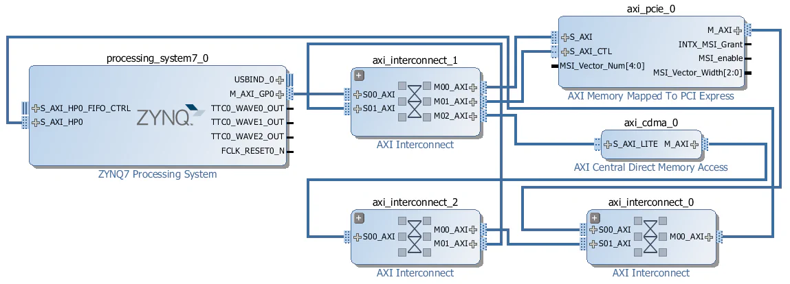
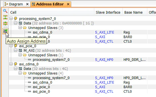
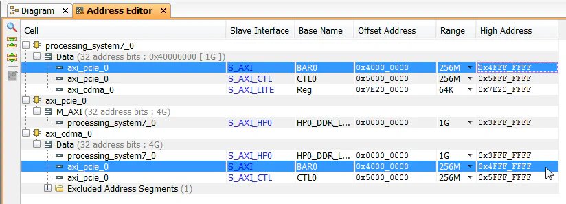
So again let’s look at who the bus masters are and what address spaces they can access:
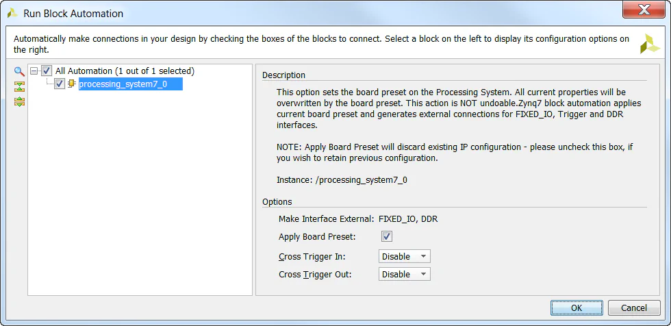
The first thing we have to do is provide the PicoZed board definition files to our Vivado installation so that the PicoZed will show up in the list of targets when we create a new project. The board definition files contain information about the hardware on the target board and also on how the Zynq PS should be configured in order to properly connect to that hardware.
picozed_7030_fmc2 into the folder C:\Xilinx\Vivado\2015.4\data\boards\board_files of your
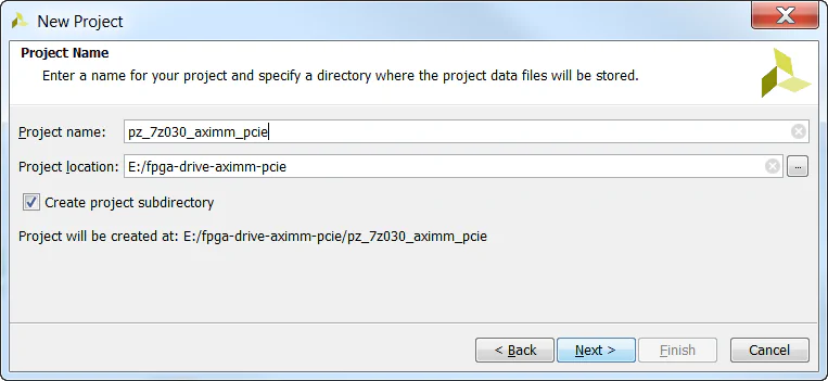
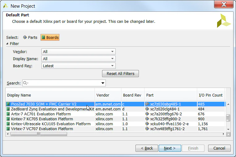
Vivado installation.Let’s kick off the design by creating a new project in Vivado and selecting the PicoZed 7Z030 as our target.
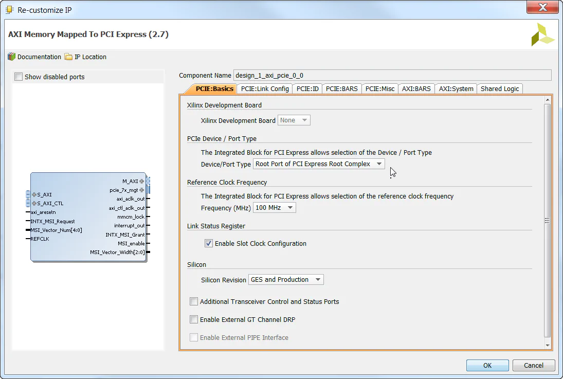
In the following steps, we’ll create the block design then add the Zynq PS and the AXI Memory Mapped PCI Express Bridge.
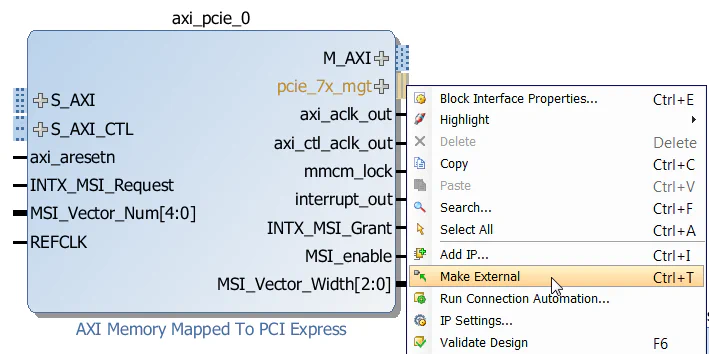
Our design will be using the two clocks supplied by the
AXI-PCIe bridge: axi_aclk_out and axi_ctl_aclk_out. We will need to add a Processor System Reset to generate resets for each of those clocks.
From the IP Catalog, add a “Processor System Reset” to the design - this one should automatically be called proc_sys_reset_0.
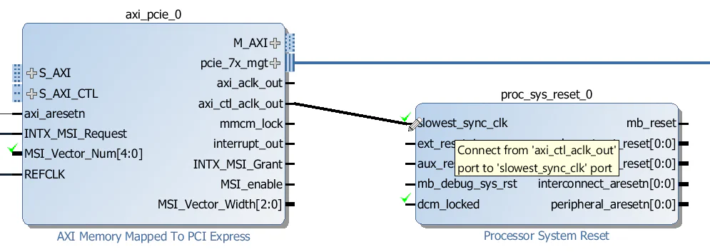
Connect the axi_ctl_aclk_out output of the AXI-PCIe block to the slowest_sync_clk input of the proc_sys_reset_0 Processor System Reset.
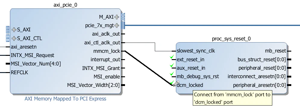
Connect the mmcm_lock output of the AXI-PCIe block to the dcm_locked input of the proc_sys_reset_0 Processor System Reset.
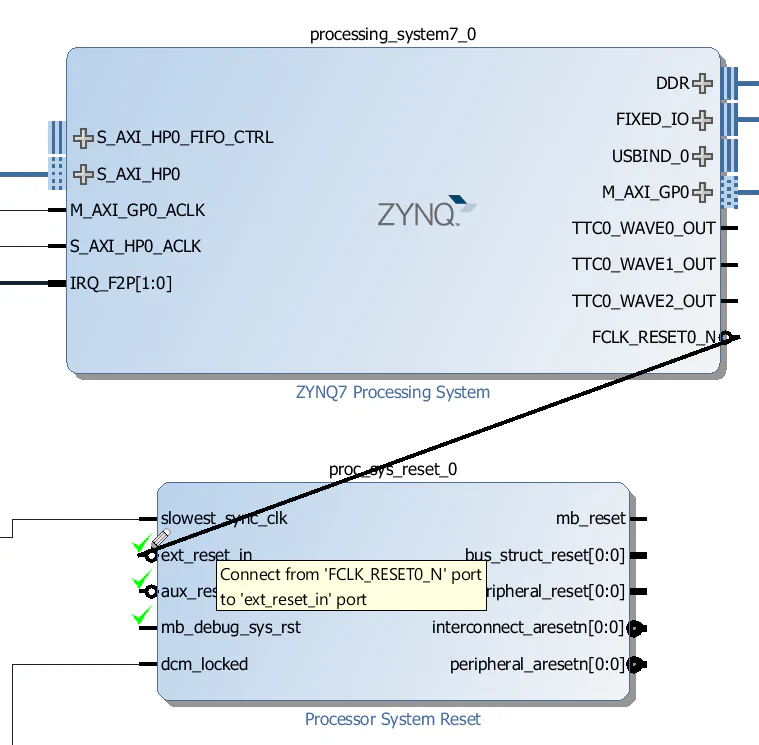
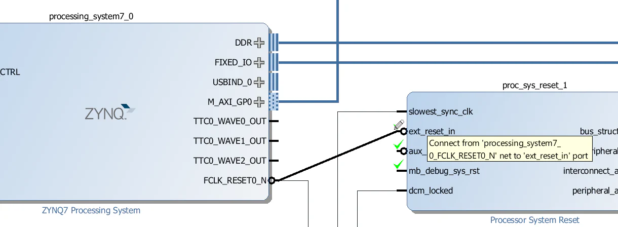
Connect the FCLK_RESET0_N output of the Zynq PS to the ext_reset_in input of the proc_sys_reset_0 Processor System Reset.
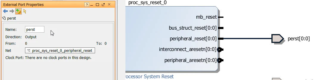
Right click on the peripheral_reset output of the proc_sys_reset_0 Processor System Reset and click “Make External”. This will be the signal that drives the PCIe reset (PERST) input of the SSD.
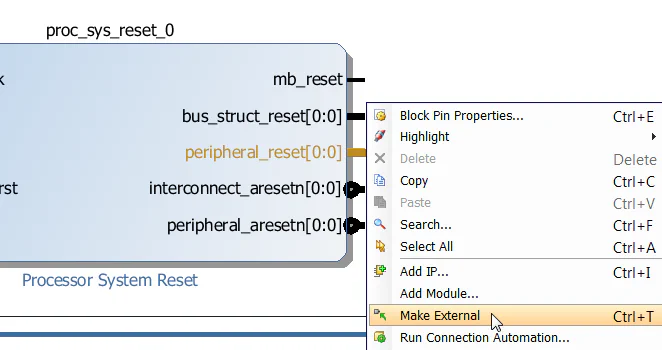
Click on the port we just created and rename it to “perst”.
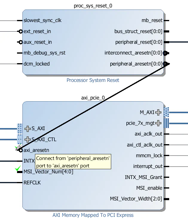
Connect the peripheral_aresetn output of proc_sys_reset_0 to the axi_aresetn input of the axi_pcie_0 block.
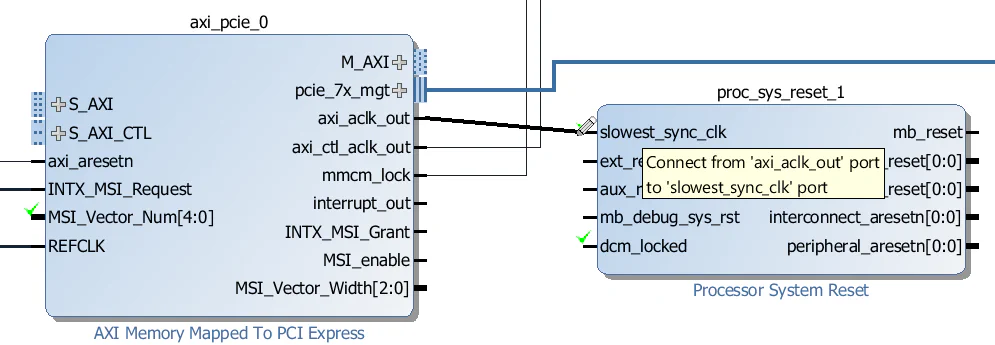
From the IP Catalog, add another “Processor System Reset” to the design - this one should automatically be called proc_sys_reset_1.
Connect the axi_aclk_out output of the AXI-PCIe block to the slowest_sync_clk input of the proc_sys_reset_1 Processor System Reset.
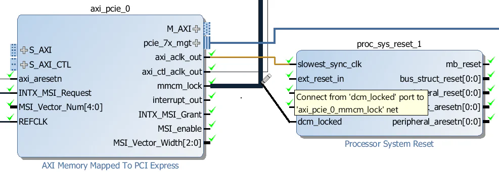
Connect the mmcm_lock output of the AXI-PCIe block to the dcm_locked input of the proc_sys_reset_1 Processor System Reset.
Connect the FCLK_RESET0_N output of the Zynq PS to the ext_reset_in input of the proc_sys_reset_1 Processor System Reset.
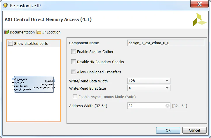
We’re going to add a Central DMA to this design to allow us to make DMA transfers between the PCIe end-point and the DDR3 memory. We won’t actually test it, that will be the subject of another tutorial, but most PCIe designs can benefit from having a Central DMA because it allows for higher throughput over the PCIe link using burst transfers.
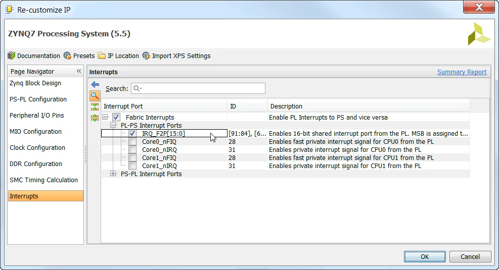
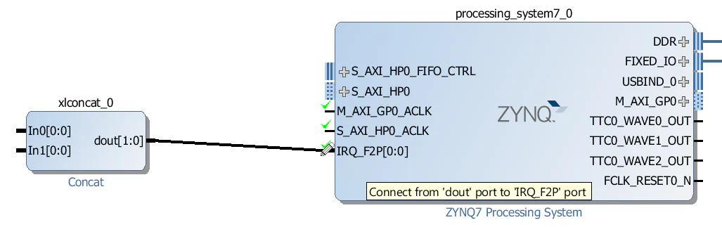
To connect interrupts to the IRQ_F2P port of the Zynq PS, we need to use a Concat.
IRQ_F2P port of the Zynq PS.
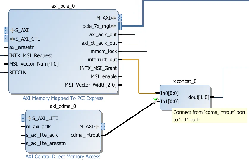
interrupt_out output of the AXI-PCIe block to the “In0” input of the Concat.cdma_introut output of the CDMA block to the “In1” input of the Concat.
Now the last thing to do is add the AXI Interconnects and wire up all the AXI interfaces.
axi_interconnect_0:
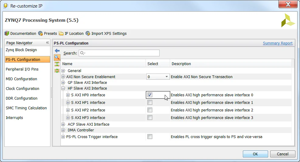
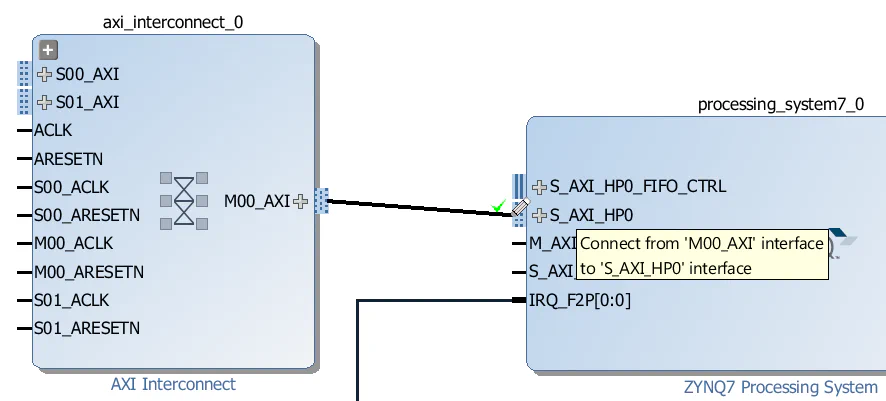
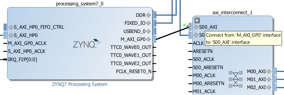
axi_interconnect_0. We’ll use this to create two ports for accessing the DDR3 memory.M00_AXI port of the axi_interconnect_0 to the S_AXI_HP0 port of the Zynq PS.
axi_interconnect_1:
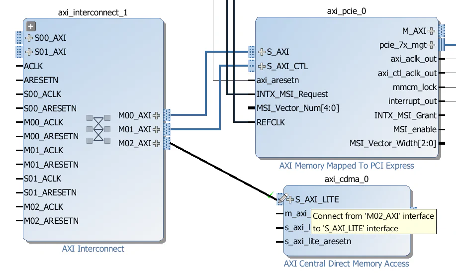
axi_interconnect_1. We’ll use this to create two ports for accessing the AXI-PCIe control interface, the PCIe end-point and the CDMA control interface.M00_AXI port of the axi_interconnect_1 to the S_AXI port of the AXI-PCIe block.M01_AXI port of the axi_interconnect_1 to the S_AXI_CTL port of the AXI-PCIe block.M02_AXI port of the axi_interconnect_1 to the S_AXI_LITE port of the CDMA block.
axi_interconnect_2:
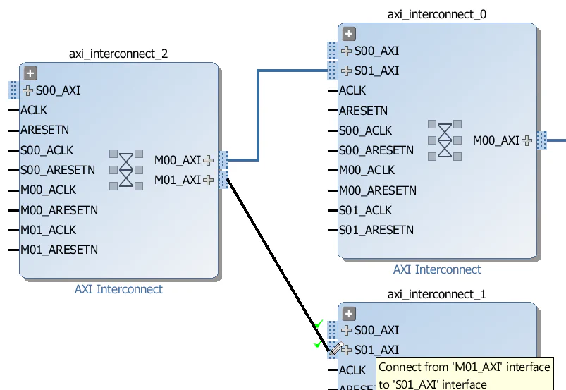
axi_interconnect_2. We’ll use this to allow the CDMA to access both the DDR3 memory and the PCIe end-point.M00_AXI port of the axi_interconnect_2 to the S01_AXI port of the axi_interconnect_0 (the first interconnect we created).M01_AXI port of the axi_interconnect_2 to the S01_AXI port of the axi_interconnect_1 (the second interconnect we created).
Now for the rest of the connections:
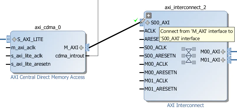
M_AXI port of the CDMA block to the S00_AXI port of the axi_interconnect_2.
M_AXI_GP0 port of the Zynq PS to the S00_AXI port of the axi_interconnect_1.
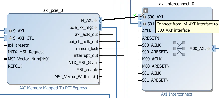
M_AXI port of the AXI-PCIe block to the S00_AXI port of the axi_interconnect_0.
Let’s start by hooking up the main clock axi_aclk_out:
axi_aclk_out clock to the M_AXI_GP0_ACLK and S_AXI_HP0_ACLK inputs of the Zynq PS.axi_aclk_out clock to the m_axi_aclk and s_axi_lite_aclk inputs of the CDMA.axi_aclk_out clock to the “ACLK”, S00_ACLK, M00_ACLK and S01_ACLK inputs of the axi_interconnect_0 (ie. all of the clock inputs).axi_aclk_out clock to the “ACLK”, S00_ACLK, M00_ACLK, S01_ACLK and M02_ACLK inputs of the axi_interconnect_1 (notice that we do not connect M01_ACLK yet!).axi_aclk_out clock to the “ACLK”, S00_ACLK, M00_ACLK and M01_ACLK inputs of the axi_interconnect_2 (ie. all of the clock inputs).Now the control clock axi_ctl_aclk_out:
axi_ctl_aclk_out clock to the M01_ACLK input of the axi_interconnect_1.
interconnect_aresetn output of the proc_sys_reset_1 Processor System Reset to the “ARESETN” input of ALL 3 AXI Interconnects.peripheral_aresetn output of the proc_sys_reset_1 Processor System Reset to the following inputs:s_axi_lite_aresetnS00_ARESETN, M00_ARESETN and S01_ARESETNS00_ARESETN, M00_ARESETN, S01_ARESETN and M02_ARESETN (notice that we do not connect M01_ARESETN yet!)S00_ARESETN, M00_ARESETN and M01_ARESETNperipheral_aresetn output of the proc_sys_reset_0 Processor System Reset to the M01_ARESETN of axi_interconnect_1.
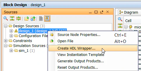
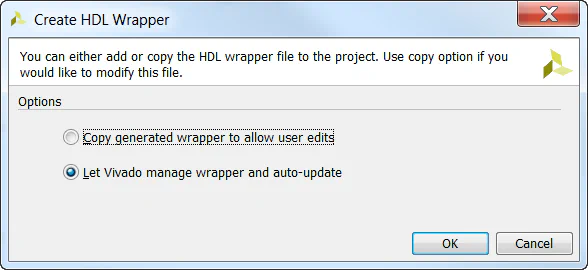
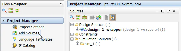
Now the block diagram is complete, so we can save it and create a HDL wrapper for it.
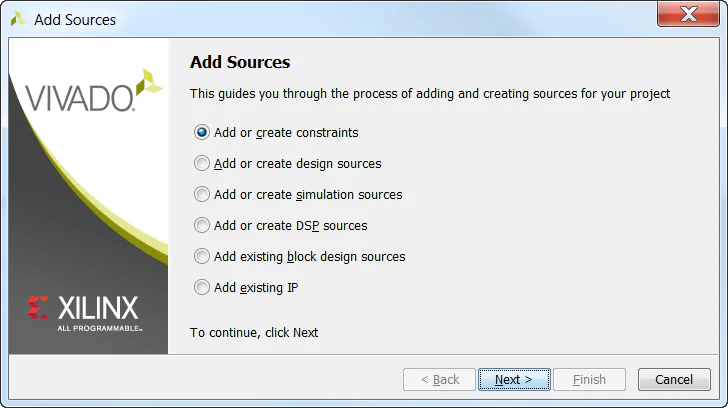
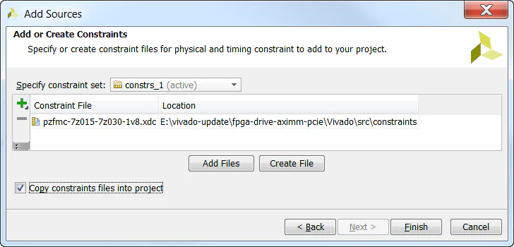
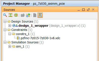
We must now add our constraints to the design for assignment of the PCIe integrated block, the gigabit transceivers, the reference clocks and a few other signals.
You’re all done!
In the next and final part of this tutorial series, we will test our design on hardware by connecting an NVMe PCIe SSD to our FPGA. We’ll start by running a simple stand-alone application that will check the PCIe bus status and enumerate the end-points. Then we’ll generate a PetaLinux build that is customized to our hardware and we’ll bring up the SSD from the command line.
The sources for re-generating this project automatically can be found on Github here: FPGA Drive PCIe Root Complex design
Here are some other useful resources for creating PCI Express designs:
If you have any questions about this tutorial, or if you run into problems, please leave me a comment below.