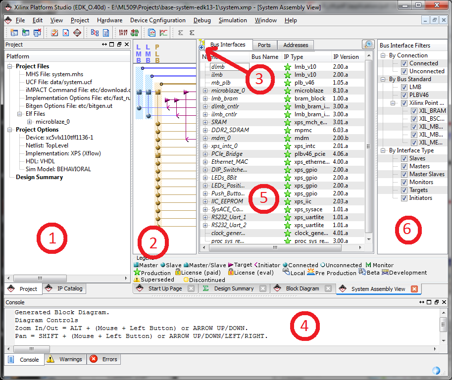
The diagram below shows the EDK window with an open project. The important areas are labelled with numbers 1 to 6.

1. Project Information
This area contains information about the project and contains two tabs: Project and IP Catalog.
- The Project tab lists the project files and also some of the project settings such as target FPGA.
- The IP catalog contains a list of the peripherals or IP cores that your project has access to. You will use this tab when you want to instantiate IP cores into your design. Get information about cores by right clicking on them and clicking “View PDF datasheet”.
2. Bus connectivity
This area shows the interconnections between your IP cores, your memory and the Microblaze processor(s). You’ll notice two types of bus: the Processor Local Bus (PLB) and the Local Memory Bus (LMB).
The filled circles and squares you see on the bus lines indicate connections. For example, the filled circle to the left of IIC_EEPROM indicates that it is connected to the PLB. If you click on the circle, you can disconnect it from the PLB and the circle becomes hollow.
3. View Buttons
Although this looks like one button, it is actually two buttons. Click on the top of this little icon and you can change between hierarchical view and flat view. Try it yourself to see the difference however I personally never use the flat view.
4. Console Window
The console window displays all the textual information, warnings and errors that occur as you make changes to the project, generate netlists, bitstreams, etc.
5. System Assembly View
This is where all your project’s IP cores and processors are listed. Anything you use in your design will be listed here and you typically place things here from the IP catalog or by modifying your MHS file.
The Bus Interface tab shows the following information for each core:
- Instance name - this name is what you will use to reference the core in your UCF constraints file.
- Bus name - the bus to which the core is connected (eg. PLB).
- IP type - the name of the IP core as in the IP catalog. This column also shows an icon that indicates whether this IP core is in development or if it is a final revision (green star). The cores in development will always be checked for code changes every time you try to build the project.
- IP version - the version of the IP core.
The Ports tab shows the user accessible ports of the IP cores and the nets to which they connect. The first item in the Ports tab is the external ports which is the list of ports that will be connected to external pins of the FPGA. You create external ports by using the “Make External” option in the net drop-down menus, or by modifying your MHS file.
The Addresses tab shows how the IP cores are mapped to the PLBs in your design (usually you only have one PLB). The mapping is important to the Microblaze processor(s) because it uses these addresses to communicate with the cores, by reading and writing to registers inside the cores. The “Generate addresses” button allows you to create new addresses for cores that you manually added to the design (ie. for cores that Base System Builder did not include for you).
6. Filters Pane
The filters pane allows you to filter what is shown in the System Assembly View, for the case that you have many IP cores in your design or you want a simplified view of your design. I personally never find myself using this.