December 20, 20217 minutes
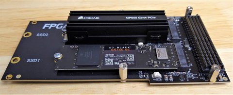
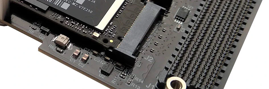
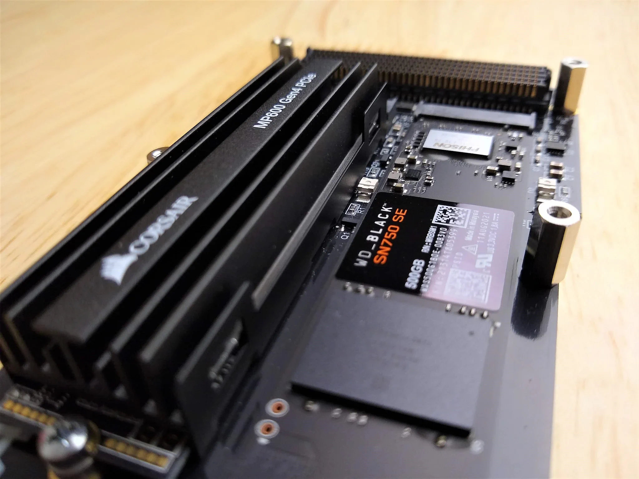
One of the projects I’ve been working on in the last few months has been upgrading our M2 SSD to FPGA adapter product ( FPGA Drive FMC) to support the new Gen4 PCIe SSDs. It’s now available to buy so I thought that I would share some photos and write a bit about the changes that we made. The photos were taken with these two Gen4 PCIe SSDs:
Perhaps the most influential change to the PCB design was the change of board material. The original FPGA Drive FMC product was made with standard FR4 PCB laminate and it was designed to support up to PCIe Gen3 which operates at 8GHz. When we go up to PCIe Gen4, the signal frequency doubles to 16GHz, and we cross over a point where the losses of the FR4 laminate become a bit too high for operating reliable error-free serial links of a decent length.
There are quite a few options for low-loss PCB materials, all of them considerably more expensive than FR4. We decided to go with Megtron-6 which has excellent specs and also happens to be a popular choice for many of the Xilinx Development boards.
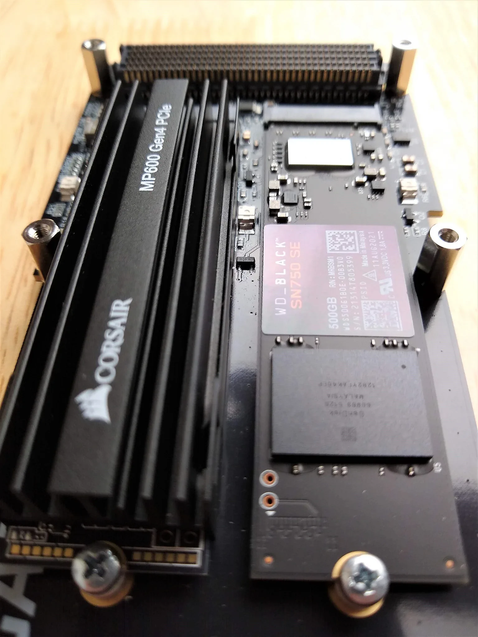
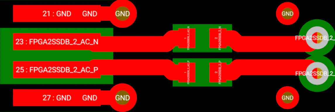
In high frequency designs, the way traces are layed out has an enormous influence on signal integrity. It’s very important to optimize all high frequency traces including their transitions to connectors and components. PCIe uses AC-coupled serial links, so the trace work around the AC coupling capacitors can be an important source of losses and reflections. In the original design we used 0.1uF ceramic capacitors in the 0402 package and the image below shows how the routing was done. The rectangular pads on the left are the pins of the M2 connector, the pads in the middle of the image are the capacitor pads, while the circles are via pads.
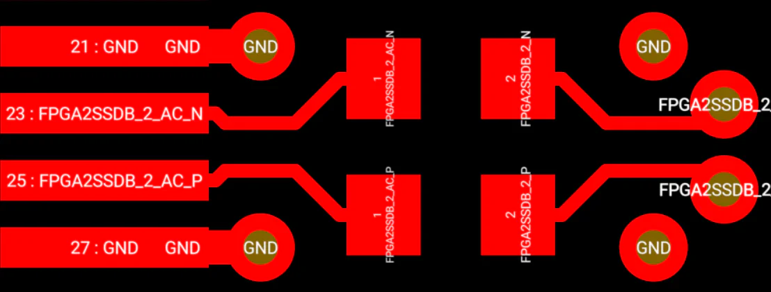
In the new version (shown below), we used 0.22uF ceramic capacitors in the smaller 0201 package. By using capacitors in a smaller package, the traces can be more streamlined, with only a slight bend that is required to keep those capacitors apart enough to prevent assembly issues. Note that the traces are wider in the new design; this is due to the change of PCB substrate. The Megtron-6 material has a different dielectric constant than FR4, requiring wider traces to maintain the 85 ohm trace impedance.
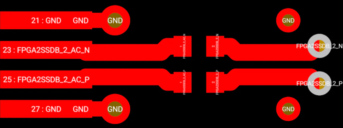
In the image below you can see the 0201 AC coupling capacitors sitting between the M2 connector and the FMC connector.
In both versions, we actually cut voids in the ground plane immediately below the top-layer pads of the capacitors. This reduces losses caused by the capacitor’s pads coupling signal directly to the ground plane below them. You can see this represented by the green patches in the images below.

Notice that we also cut voids underneath the pads of the M2 connector.
When I did some testing of our original FR4 design at 16GHz, it was interesting to notice that the worst performing lanes were typically the longest ones and the ones with the most bends. Intuitively you can understand that the longer the trace, the higher the loss, but it wasn’t so obvious to me at the time that the bends would also be such an important contributor to the losses.
In the new design, we’ve tightened up the trace work to shorten the links and remove as many turns and bends as possible. Fortunately in PCIe, while the +/- signals of a differential pair must be kept tightly matched, there is no requirement for length matching between lanes. This means that each lane can be layed out to minimize length, without concern for the length of the other lanes.
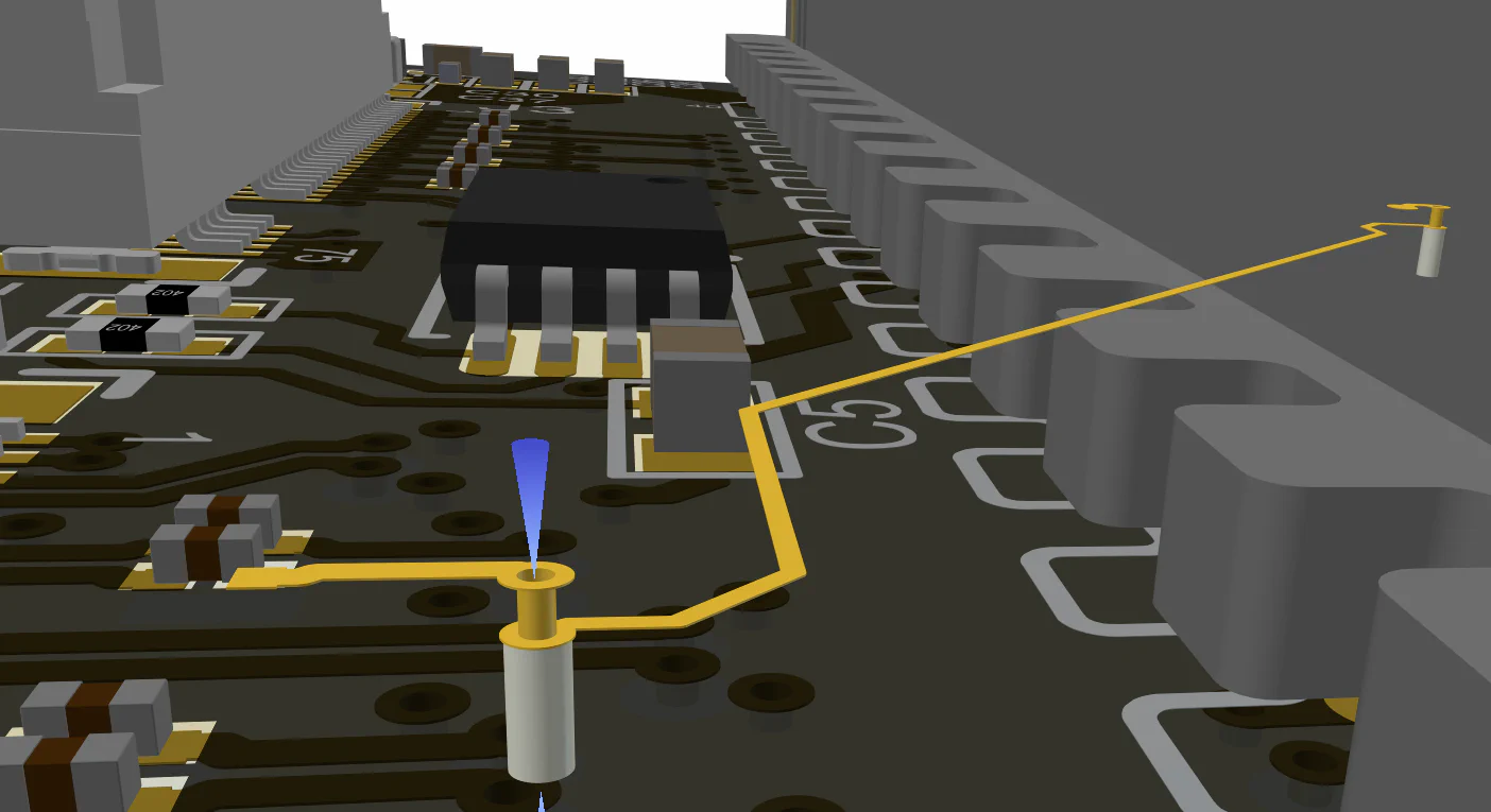
Another improvement we’ve made to the trace work is the use of back-drilling to remove all of the stubs created by vias on the PCIe traces. In back drilling, the PCB manufacturer basically drills out the unused ends of the high frequency signal vias (ie. the end of the via that doesn’t serve in sending the signal to another layer because the signal has already reached the layer it needs to be on). The image below illustrates one signal that goes from the top layer, through a via to an internal signal layer, and then back up to the top layer through another via at another location of the board. The grey cylendars are the sections of the vias that are drilled out, and they go from the bottom layer to the inner signal layer. Those unused sections of the vias can act as antennas and hence contribute to signal loss.
When upgrading a board for higher frequencies, you also have to go through all of the connectors in the design and make sure that they are specified to work at the intended frequencies.
For the SAMTEC FMC connector, we can check their high speed characterization report for the 10mm mated height, and we see that there is no issue at 16GHz.
In the case of the M2 connector ( 1-2199230-6), we couldn’t get the same data from the manufacturer TE Connectivity 1. So, we decided to go with an M2 connector that was officially specified to support Gen4: the MDT420M02003 from Amphenol. Luckily, the footprint of the Amphenol connector is the same.

The new boards have a logo with a “Gen4” superscript. Although these boards haven’t yet been tested for Gen5 frequencies, they might actually be compliant so I might end up regretting this change! Either way, I wanted these new boards to be easily distinguished from the original boards.
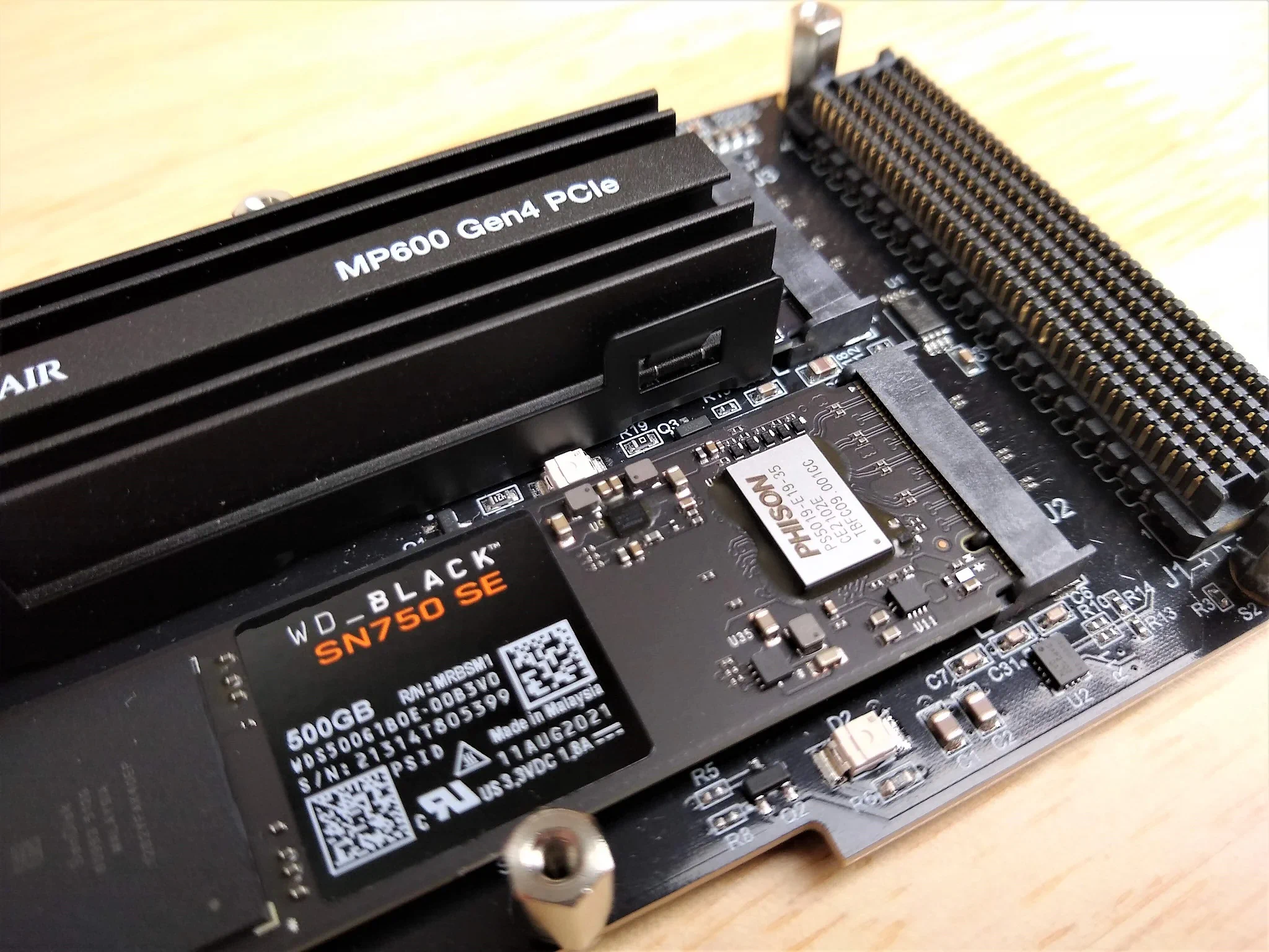
These new Gen4 SSDs generally have much better read and write performances than their Gen3 equivalents. For example, take a look at this comparison between the Samsung 970 PRO and the Samsung 980 PRO:
| SSD | Interface | Sequential Reads | Sequential Writes |
|---|---|---|---|
| Samsung 970 PRO | PCIe Gen3 | Up to 3,500 MB/s | Up to 2,700 MB/s |
| Samsung 980 PRO | PCIe Gen4 | Up to 7,000 MB/s | Up to 5,000 MB/s |
Based on manufacturers specs, the performance improvement is very impressive; but be careful. If you’re using them with an FPGA, you’ll only benefit from the increased performance if you have the right setup. Here are the important points to get right if you don’t want a bottleneck to eat up all of those gains:
| Xilinx device | Integrated blocks | Support notes |
|---|---|---|
| Virtex Ultrascale+ HBM | PCIE4C | PCIE4C supports Gen4 with some unsupported features |
| Virtex Ultrascale+ 58G | PCIE4C | PCIE4C supports Gen4 with some unsupported features |
| Versal ACAP | PL PCIE4 | PL PCIE4 blocks are fully compliant to PCIe Gen4 |
TE Connectivity did send me an email confirming that their connector ( 1-2199230-6) would support PCIe Gen4, but they didn’t have an official document stating this. ↩︎