When designing a network tap on an FPGA, the logical place to start is the pass-through between two Ethernet ports. In this article, I’ll discuss a convenient way to connect two Ethernet ports at the PHY-MAC interface, which will form the basis of a network tap. The pass-through will be designed in Vivado for the ZedBoard combined with an Ethernet FMC. In future articles, I’ll discuss other aspects of an FPGA network tap design, including monitor ports, packet filtering, and opportunities for hardware acceleration in the FPGA.
Pass-through at the MAC interface (GMII, RGMII or SGMII)
The criteria for an ideal pass-through are:
- it must be completely transparent to all devices communicating over the link,
- it must preserve the fidelity of the link, and ideally,
- it should add very little latency to the link.
From those criteria we could suppose that if we could simply tap the wires of the Ethernet cable, we’d have our ideal tap. Unfortunately, due to the complexity of Gigabit Ethernet signals, we can’t do that, instead we have to break the link and connect each end to it’s own Ethernet PHY. The pass-through is implemented on the other end of the PHYs, or the MAC interface which is typically one of the following standards: GMII, RGMII or SGMII. In the case of the Ethernet FMC, which uses 4x Marvell 88E1510 Ethernet PHYs, we’re dealing with the RGMII interface.
RGMII signals are double-data-rate (DDR) and so in order to bring the data into our FPGA fabric and send it back out, we need to use the IDDR and ODDR primitives. Fortunately, there is an IP that implements the RGMII interface for us and provides us with a single-data-rate interface which we can use for the pass-through and for “tapping”. The GMII-to-RGMII IP core, included with Vivado, converts an RGMII interface, to a GMII interface. To implement our pass-through, all we have to do is instantiate two GMII-to-RGMII converters, route them to two separate Ethernet PHYs and loop together the two GMII interfaces.

The block diagram above illustrates the general idea. Port 0 and port 1 of the Ethernet FMC are each connected to a GMII-to-RGMII converter, and the GMII interfaces are passed through to the opposite port.
Use FIFOs to connect the GMII interfaces
When connecting one GMII interface to another, you will notice that the transmit interface has a separate clock to the receive interface. The GMII TX data, TX enable and TX error signals are all synchronous to the TX clock, whereas the GMII RX data, RX valid and RX error signals are all synchronous to the RX clock. So you can’t directly connect the GMII transmit interface to the GMII receive interface - you have to use proper clock domain crossing. The easy way to do that is by using a FIFO with independent read and write clocks - you’ll need two of them, one for each direction of data flow.

Wire the FIFOs as elastic buffers
The natural way to connect FIFOs to the transmit and receive interfaces is to use the rx_dv (RX valid) output of the GMII interfaces to drive the “write enable” inputs of the FIFOs, and to use the “valid” output of the FIFOs to drive the tx_en (TX enable) inputs of the GMII interface. However, in our application, there is a problem with this method. If even momentarily the FIFO is being read slightly faster than it is being written to, you will have occasions where the FIFO is empty for one clock cycle and forced to de-assert the “valid” signal. This is a problem because the GMII interface “enable” and “valid” signals are only supposed to be de-asserted at the end of a packet, so this gap effectively terminates the Ethernet packet that you are feeding to the PHY. The better solution is to feed the “enable” and “valid” signals through the FIFOs, and to design the FIFOs as elastic buffers. Remember that once you decide that a FIFO will be written to and read from constantly, using two independent clocks, it must be designed as an elastic buffer or you risk losing data due to the FIFO reaching the full or empty state. In the elastic buffer solution, we still use our tx_en and rx_dv signals, but we use them to determine what data the elastic buffer can discard at the write interface (when it’s too full), as well as when the elastic buffer can momentarily halt the read interface (when it’s too empty). An elastic buffer is not perfect and it relies on a certain amount of redundancy being present in the data, but in typical Ethernet applications, there is enough time between packets that the job of designing a reliable elastic buffer is quite simple.
So when you want to wire up a FIFO as a simple elastic buffer, there are two things to setup:
1. Programmable full and empty outputs
These signals will tell us when the FIFOs are too full or too empty and they allow us to keep the FIFO occupancy within a certain range. Typically that “range” is centered at the mid-point of the FIFO, for example, if our FIFO contains 1000 words, then we could set our desired occupancy to be between 400 and 600. In this case, the programmable full output would be set to 600, and the programmable empty output would be set to 400.
2. Write enable and read enable logic
The write and read enable inputs must be connected to logic functions that will throttle the FIFO, filling it up when it gets too empty and emptying it when it gets too full. The functions are:
- write enable <= NOT prog_full OR rx_valid
- read enable <= NOT prog_empty OR tx_valid

Configuring the GMII-to-RGMII converter
For the GMII-to-RGMII converter to operate properly, we have to let it know the actual link speed that was setup by the PHY during auto-negotiation. But how do we communicate this information to the core?
You may have noticed that the GMII-to-RGMII core contains two MDIO ports, one of which is normally connected to the MAC, and the other which is normally externalized and connected to the PHY. The GMII-to-RGMII core “sits” on the MDIO bus, as though it were another PHY, and it can be configured over that MDIO bus. So we communicate the link speed information to the core over the MDIO bus and the typical sequence is as follows:
- Trigger the auto-negotiation sequence in the PHY (optional)
- We read the actual link speed from the PHY after auto-negotiation has completed
- We write the actual link speed to the GMII-to-RGMII core
The last step involves writing to a specific register within the GMII-to-RGMII core with a value that corresponds to the link speed. To do this we need the address of the register to write to (0x10) and the “PHY” address of the GMII-to-RGMII core (I quote the word PHY because the core is not a PHY). The “PHY” address of the GMII-to-RGMII core is specified in Vivado, and is 8 by default. In order to communicate with two GMII-to-RGMII cores in our design, we have connected one of the MDIO “inputs” to GEM1 of the Zynq PS. We then connected the MDIO “output” to the MDIO “input” of the second GMII-to-RGMII converter (see block diagram above). This way, we can configure both GMII-to-RGMII converters using only the MDIO port of GEM1. In Vivado, we configure the GMII-to-RGMII cores to have different “PHY addresses”, specifically 7 and 8, so that we don’t create a bus conflict.

Depending on the established link speed, we need to write the following values to register 0x10 of both of the GMII-to-RGMII converters:
- For a link speed of 1Gbps, we need to write 0x140.
- For a link speed of 100Mbps, we need to write 0x2100.
- For a link speed of 10Mbps, we need to write 0x100.
For reliable operation, the link on Port 0 should be the same speed as that on Port 1, ie. don’t try to use this pass-through to connect networks of different speeds.
Sources Git repository
The sources for re-generating this project automatically can be found on Github at the link below.
Ethernet FMC Network Tap Github Source Code
If you want to better understand how the sources are organized, you can read this post: Version control for Vivado projects.
Next on the FPGA network tap
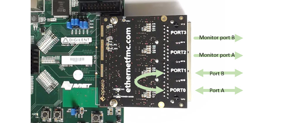
In the next post on the FPGA network tap, we’ll hook up the other two ports of the Ethernet FMC as monitor ports which will enable “listening” by a third device. Port 2 will send a copy all packets going in one direction, while port 3 will send a copy of all packets going in the other direction, so the result will be a full gigabit network tap. We’ll also hook the ports up to soft TEMAC IPs and look at filtering the packets within the FPGA fabric.