Title here
Summary here
Bringing up NVMe SSDs on the Versal VCK190 with FPGA Drive FMC Gen4 and PetaLinux
March 18, 202422 minutes

High-capacity non-volatile storage is pretty handy in the intensive computing applications that the Versal ACAP adaptive SoCs get employed in. NVMe SSDs are a perfect way to provide that storage because they can directly interface with the Versal’s integrated blocks for PCIe. Those integrated blocks are Gen4 compliant which makes for an extremely high bandwidth connection between the FPGA fabric and the storage medium.
Over the past couple of weeks, my team and I have been bringing up an NVMe SSD on the Versal AI Core VCK190 Evaluation kit using the FPGA Drive FMC Gen4 adapter. We’ve built a new reference design from our work and shared it on Github. In this post we’ll look at how you can build and run the example design, and then we’ll partition and write a file to one of the SSDs. For those who are trying to do this from scratch using the QDMA Subsystem for PCIe IP, Vivado and PetaLinux, the last half of this post will be about the things that we found to be important in getting everything working correctly.
Alternatively, you can use version 2023.2 of the tools and checkout the corresponding branch of the Git repository.
The VCK190 and VMK180 are not supported by the free version of the AMD Xilinx tools, but you can download an evaluation license that will allow you to build these projects.
These are the instructions for building the design from sources. If you just want to try it out on hardware, you can download the pre-built boot files from the table below.
On a Linux machine (physical or virtual), source the Vivado and PetaLinux 2022.1 tools:
source <path-to-vivado-install>/2022.1/settings64.sh
source <path-to-petalinux-install>/2022.1/settings.sh
Clone the repo:
git clone https://github.com/fpgadeveloper/fpga-drive-aximm-pciedev-v2023.2 of that repository.
If the branch no longer exists, we’ve probably made it a release with tag v2023.2.Build the target design:
cd fpga-drive-aximm-pcie/PetaLinux
make petalinux TARGET=vck190_fmcp1
In the above example we’re building the vck190_fmcp1 target design, but you can choose from these other Versal designs too:
| Target design | Board | SSD slots | FMC Connector | Pre-built boot files |
|---|---|---|---|---|
vck190_fmcp1 | VCK190 | 2 | FMCP1 | Files or Disk image |
vck190_fmcp2 | VCK190 | 2 | FMCP2 | Files or Disk image |
vmk180_fmcp1 | VMK180 | 2 | FMCP1 | Files or Disk image |
vmk180_fmcp2 | VMK180 | 2 | FMCP2 | Files or Disk image |
Connector locations:
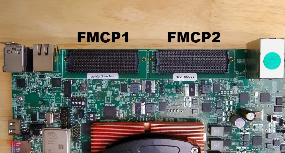
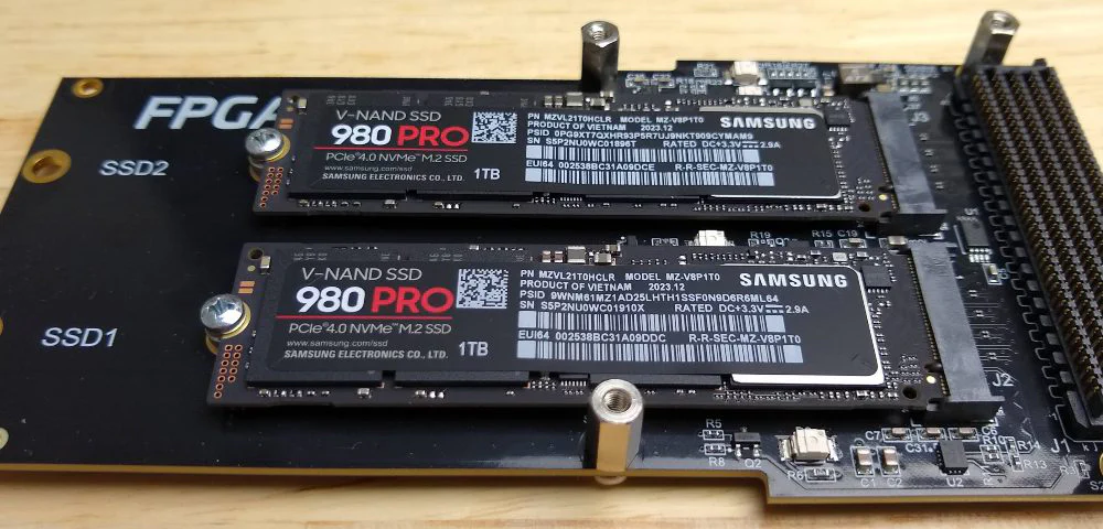
Attach two SSDs to the FPGA Drive FMC Gen4. I’m using two Samsung 980 PROs because they can support PCIe Gen4.
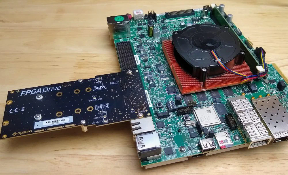
Attach the FPGA Drive FMC Gen4 to FMCP1 of the VCK190 board (or the connector of your chosen target design).
Connect the power supply to the VCK190/VMK180 board and the USB cable. The other end of the USB cable should be connected to a PC with a UART terminal program.
Copy the boot files to the SD card as described here: Prepare the SD card. The easier way is to download the disk image and use Win32DiskImager to write the SD card (it must be at least 16GB in size).
Plug the SD card into the VCK190/VMK180 Versal SD card slot. Note that the VCK190/VMK180 board has two SD card slots, one for the Versal configuration and the other for the system controller (Zynq UltraScale+). The Versal SD card slot is the one that is on the top/component side of the board (you can see mine in the bottom right corner of the image above, the card is red and grey). You can leave the system controller SD card slot empty.
Open up a terminal console such as Putty and configure it for the UART port of the VCK190/VMK180 board. The baud rate should be set to 115200 bps.
Power up the board and wait for the PetaLinux boot sequence to complete. The parts of the boot log that are related to PCIe should look as below:
[    4.697756] xilinx-xdma-pcie 80000000.qdma: host bridge /amba_pl@0/qdma@400000000 ranges:
[    4.705999] xilinx-xdma-pcie 80000000.qdma:   No bus range found for /amba_pl@0/qdma@400000000, using [bus 00-ff]
[    4.716345] xilinx-xdma-pcie 80000000.qdma:      MEM 0x00a8000000..0x00afffffff -> 0x00a8000000
[    4.725192] xilinx-xdma-pcie 80000000.qdma: PCIe Link is UP
[    4.730894] xilinx-xdma-pcie 80000000.qdma: PCI host bridge to bus 0000:00
[    4.737818] pci_bus 0000:00: root bus resource [bus 00-ff]
[    4.743338] pci_bus 0000:00: root bus resource [mem 0xa8000000-0xafffffff]
[    4.750285] pci 0000:00:00.0: [10ee:b0b4] type 01 class 0x060400
[    4.756339] pci 0000:00:00.0: reg 0x10: [mem 0x00000000-0xffffffff 64bit pref]
[    4.763652] pci 0000:00:00.0: PME# supported from D3cold
[    4.769530] pci 0000:00:00.0: bridge configuration invalid ([bus 00-00]), reconfiguring
[    4.777655] pci 0000:01:00.0: [144d:a80a] type 00 class 0x010802
[    4.783723] pci 0000:01:00.0: reg 0x10: [mem 0x00000000-0x00003fff 64bit]
[    4.791204] pci_bus 0000:01: busn_res: [bus 01-ff] end is updated to 01
[    4.797872] pci 0000:00:00.0: BAR 0: no space for [mem size 0x100000000 64bit pref]
[    4.805587] pci 0000:00:00.0: BAR 0: failed to assign [mem size 0x100000000 64bit pref]
[    4.813650] pci 0000:00:00.0: BAR 8: assigned [mem 0xa8000000-0xa80fffff]
[    4.820484] pci 0000:01:00.0: BAR 0: assigned [mem 0xa8000000-0xa8003fff 64bit]
[    4.827846] pci 0000:00:00.0: PCI bridge to [bus 01]
[    4.832842] pci 0000:00:00.0:   bridge window [mem 0xa8000000-0xa80fffff]
[    4.839729] xilinx-xdma-pcie 90000000.qdma: host bridge /amba_pl@0/qdma@440000000 ranges:
[    4.847969] xilinx-xdma-pcie 90000000.qdma:   No bus range found for /amba_pl@0/qdma@440000000, using [bus 00-ff]
[    4.858310] xilinx-xdma-pcie 90000000.qdma:      MEM 0x00b0000000..0x00bfffffff -> 0x00b0000000
[    4.867132] xilinx-xdma-pcie 90000000.qdma: PCIe Link is UP
[    4.872823] xilinx-xdma-pcie 90000000.qdma: PCI host bridge to bus 0001:00
[    4.879745] pci_bus 0001:00: root bus resource [bus 00-ff]
[    4.885266] pci_bus 0001:00: root bus resource [mem 0xb0000000-0xbfffffff]
[    4.892200] pci 0001:00:00.0: [10ee:b0b4] type 01 class 0x060400
[    4.898257] pci 0001:00:00.0: reg 0x10: [mem 0x00000000-0xffffffff 64bit pref]
[    4.905565] pci 0001:00:00.0: PME# supported from D3cold
[    4.911417] pci 0001:00:00.0: bridge configuration invalid ([bus 00-00]), reconfiguring
[    4.919538] pci 0001:01:00.0: [144d:a80a] type 00 class 0x010802
[    4.925602] pci 0001:01:00.0: reg 0x10: [mem 0x00000000-0x00003fff 64bit]
[    4.933080] pci_bus 0001:01: busn_res: [bus 01-ff] end is updated to 01
[    4.939743] pci 0001:00:00.0: BAR 0: no space for [mem size 0x100000000 64bit pref]
[    4.947453] pci 0001:00:00.0: BAR 0: failed to assign [mem size 0x100000000 64bit pref]
[    4.955516] pci 0001:00:00.0: BAR 8: assigned [mem 0xb0000000-0xb00fffff]
[    4.962353] pci 0001:01:00.0: BAR 0: assigned [mem 0xb0000000-0xb0003fff 64bit]
[    4.969718] pci 0001:00:00.0: PCI bridge to [bus 01]
[    4.974712] pci 0001:00:00.0:   bridge window [mem 0xb0000000-0xb00fffff]
The parts of the boot log that are related to NVMe are shown below:
[    5.026899] nvme nvme0: pci function 0000:01:00.0
[    5.031652] pci 0000:00:00.0: enabling device (0000 -> 0002)
[    5.037368] nvme 0000:01:00.0: enabling device (0000 -> 0002)
[    5.037398] nvme nvme1: pci function 0001:01:00.0
[    5.047989] pci 0001:00:00.0: enabling device (0000 -> 0002)
[    5.053706] nvme 0001:01:00.0: enabling device (0000 -> 0002)
[    5.066021] nvme nvme0: Shutdown timeout set to 10 seconds
[    5.080704] nvme nvme1: Shutdown timeout set to 10 seconds
[    5.347560] nvme nvme1: 2/0/0 default/read/poll queues
[    5.408024] nvme nvme0: 2/0/0 default/read/poll queues
If you want to see the entire boot log, you can download it here.
Login to PetaLinux using the username petalinux. You will be asked to choose a password and then to enter it a second time.
Once you’re logged into PetaLinux, use lspci to check whether the SSDs have been detected and enumerated.
vck190-fpgadrv-2022-1:~$ lspci
0000:00:00.0 PCI bridge: Xilinx Corporation Device b0b4
0000:01:00.0 Non-Volatile memory controller: Samsung Electronics Co Ltd NVMe SSD Controller PM9A1/PM9A3/980PRO
0001:00:00.0 PCI bridge: Xilinx Corporation Device b0b4
0001:01:00.0 Non-Volatile memory controller: Samsung Electronics Co Ltd NVMe SSD Controller PM9A1/PM9A3/980PRO
We can also use the sudo lspci -vvv command to see at what speed the PCIe link has been made. We need to use sudo otherwise the
capabilities structure will be hidden. Below you will see that the Samsung 980 PRO has connected using PCIe Gen4 at 4-lanes. The
specific line reads LnkSta: Speed 16GT/s (ok), Width x4 (ok).
vck190-fpgadrv-2022-1:~$ sudo lspci -vvv
Password:
0000:00:00.0 PCI bridge: Xilinx Corporation Device b0b4 (prog-if 00 [Normal decode])
        Control: I/O- Mem+ BusMaster+ SpecCycle- MemWINV- VGASnoop- ParErr- Stepping- SERR- FastB2B- DisINTx-
        Status: Cap+ 66MHz- UDF- FastB2B- ParErr- DEVSEL=fast >TAbort- <TAbort- <MAbort- >SERR- <PERR- INTx-
<------------------ SKIPPING LINES FOR BREVITY --------------------->
0000:01:00.0 Non-Volatile memory controller: Samsung Electronics Co Ltd NVMe SSD Controller PM9A1/PM9A3/980PRO (prog-if 02 [NVM Express])
        Subsystem: Samsung Electronics Co Ltd NVMe SSD Controller PM9A1/PM9A3/980PRO
        Control: I/O- Mem+ BusMaster+ SpecCycle- MemWINV- VGASnoop- ParErr- Stepping- SERR- FastB2B- DisINTx+
        Status: Cap+ 66MHz- UDF- FastB2B- ParErr- DEVSEL=fast >TAbort- <TAbort- <MAbort- >SERR- <PERR- INTx-
        Latency: 0
        Interrupt: pin A routed to IRQ 48
        Region 0: Memory at a8000000 (64-bit, non-prefetchable) [size=16K]
        Capabilities: [40] Power Management version 3
                Flags: PMEClk- DSI- D1- D2- AuxCurrent=0mA PME(D0-,D1-,D2-,D3hot-,D3cold-)
                Status: D0 NoSoftRst+ PME-Enable- DSel=0 DScale=0 PME-
        Capabilities: [50] MSI: Enable+ Count=4/32 Maskable- 64bit+
                Address: 0000000002627000  Data: 0000
        Capabilities: [70] Express (v2) Endpoint, MSI 00
                DevCap: MaxPayload 256 bytes, PhantFunc 0, Latency L0s unlimited, L1 unlimited
                        ExtTag+ AttnBtn- AttnInd- PwrInd- RBE+ FLReset+ SlotPowerLimit 0.000W
                DevCtl: CorrErr- NonFatalErr- FatalErr- UnsupReq-
                        RlxdOrd+ ExtTag+ PhantFunc- AuxPwr- NoSnoop+ FLReset-
                        MaxPayload 128 bytes, MaxReadReq 512 bytes
                DevSta: CorrErr- NonFatalErr- FatalErr- UnsupReq- AuxPwr- TransPend-
                LnkCap: Port #0, Speed 16GT/s, Width x4, ASPM L1, Exit Latency L1 <64us
                        ClockPM+ Surprise- LLActRep- BwNot- ASPMOptComp+
                LnkCtl: ASPM Disabled; RCB 64 bytes, Disabled- CommClk-
                        ExtSynch- ClockPM- AutWidDis- BWInt- AutBWInt-
                LnkSta: Speed 16GT/s (ok), Width x4 (ok)
                        TrErr- Train- SlotClk+ DLActive- BWMgmt- ABWMgmt-
                DevCap2: Completion Timeout: Range ABCD, TimeoutDis+ NROPrPrP- LTR+
                         10BitTagComp+ 10BitTagReq- OBFF Not Supported, ExtFmt- EETLPPrefix-
                         EmergencyPowerReduction Not Supported, EmergencyPowerReductionInit-
                         FRS- TPHComp- ExtTPHComp-
                         AtomicOpsCap: 32bit- 64bit- 128bitCAS-
                DevCtl2: Completion Timeout: 50us to 50ms, TimeoutDis- LTR- OBFF Disabled,
                         AtomicOpsCtl: ReqEn-
                LnkCap2: Supported Link Speeds: 2.5-16GT/s, Crosslink- Retimer+ 2Retimers+ DRS-
                LnkCtl2: Target Link Speed: 16GT/s, EnterCompliance- SpeedDis-
                         Transmit Margin: Normal Operating Range, EnterModifiedCompliance- ComplianceSOS-
                         Compliance De-emphasis: -6dB
                LnkSta2: Current De-emphasis Level: -6dB, EqualizationComplete+ EqualizationPhase1+
                         EqualizationPhase2- EqualizationPhase3- LinkEqualizationRequest-
                         Retimer- 2Retimers- CrosslinkRes: Upstream Port
        Capabilities: [b0] MSI-X: Enable- Count=130 Masked-
                Vector table: BAR=0 offset=00003000
                PBA: BAR=0 offset=00002000
        Capabilities: [100 v2] Advanced Error Reporting
                UESta:  DLP- SDES- TLP- FCP- CmpltTO- CmpltAbrt- UnxCmplt- RxOF- MalfTLP- ECRC- UnsupReq- ACSViol-
                UEMsk:  DLP- SDES- TLP- FCP- CmpltTO- CmpltAbrt- UnxCmplt- RxOF- MalfTLP- ECRC- UnsupReq- ACSViol-
                UESvrt: DLP+ SDES+ TLP- FCP+ CmpltTO- CmpltAbrt- UnxCmplt- RxOF+ MalfTLP+ ECRC- UnsupReq- ACSViol-
                CESta:  RxErr- BadTLP- BadDLLP- Rollover- Timeout- AdvNonFatalErr-
                CEMsk:  RxErr- BadTLP- BadDLLP- Rollover- Timeout- AdvNonFatalErr+
                AERCap: First Error Pointer: 00, ECRCGenCap+ ECRCGenEn- ECRCChkCap+ ECRCChkEn-
                        MultHdrRecCap+ MultHdrRecEn- TLPPfxPres- HdrLogCap-
                HeaderLog: 00000000 00000000 00000000 00000000
        Capabilities: [168 v1] Alternative Routing-ID Interpretation (ARI)
                ARICap: MFVC- ACS-, Next Function: 0
                ARICtl: MFVC- ACS-, Function Group: 0
        Capabilities: [178 v1] Secondary PCI Express
                LnkCtl3: LnkEquIntrruptEn- PerformEqu-
                LaneErrStat: 0
        Capabilities: [198 v1] Physical Layer 16.0 GT/s <?>
        Capabilities: [1bc v1] Lane Margining at the Receiver <?>
        Capabilities: [214 v1] Latency Tolerance Reporting
                Max snoop latency: 0ns
                Max no snoop latency: 0ns
        Capabilities: [21c v1] L1 PM Substates
                L1SubCap: PCI-PM_L1.2+ PCI-PM_L1.1+ ASPM_L1.2+ ASPM_L1.1+ L1_PM_Substates+
                          PortCommonModeRestoreTime=10us PortTPowerOnTime=10us
                L1SubCtl1: PCI-PM_L1.2- PCI-PM_L1.1- ASPM_L1.2- ASPM_L1.1-
                           T_CommonMode=0us LTR1.2_Threshold=0ns
                L1SubCtl2: T_PwrOn=10us
        Capabilities: [3a0 v1] Data Link Feature <?>
        Kernel driver in use: nvme
Run lsblk to make sure that the SSDs have been recognized as block devices.
vck190-fpgadrv-2022-1:~$ lsblk
NAME        MAJ:MIN RM   SIZE RO TYPE MOUNTPOINTS
mmcblk0     179:0    0  29.7G  0 disk
|-mmcblk0p1 179:1    0     1G  0 part /run/media/mmcblk0p1
`-mmcblk0p2 179:2    0  28.7G  0 part /
nvme1n1     259:0    0 931.5G  0 disk
nvme0n1     259:1    0 931.5G  0 disk
vck190-fpgadrv-2022-1:~$
Run fdisk to create a partition on the first SSD: sudo fdisk /dev/nvme0n1.
vck190-fpgadrv-2022-1:~$ sudo fdisk /dev/nvme0n1

Welcome to fdisk (util-linux 2.37.2).
Changes will remain in memory only, until you decide to write them.
Be careful before using the write command.

Device does not contain a recognized partition table.
Created a new DOS disklabel with disk identifier 0x0acdac8a.

Command (m for help):
Type these options in fdisk:
n to create a new partitionp, then 1 to create a new primary partitionw to write the data to the diskvck190-fpgadrv-2022-1:~$ sudo fdisk /dev/nvme0n1
Welcome to fdisk (util-linux 2.37.2).
Changes will remain in memory only, until you decide to write them.
Be careful before using the write command.
Device does not contain a recognized partition table.
Created a new DOS disklabel with disk identifier 0x0acdac8a.
Command (m for help): n
Partition type
p primary (0 primary, 0 extended, 4 free)
e extended (container for logical partitions)
Select (default p): p
Partition number (1-4, default 1): 1
First sector (2048-1953525167, default 2048):
Last sector, +/-sectors or +/-size{K,M,G,T,P} (2048-1953525167, default 1953525167):
Created a new partition 1 of type 'Linux' and of size 931.5 GiB.
Command (m for help): w
The partition table has been altered.
Calling ioctl() to re-read partit[ 1888.311557] nvme0n1: p1
ion table.
Syncing disks.
vck190-fpgadrv-2022-1:~$Check the name of the partition that we just created by using lsblk. As you can see below, our partition is called nvme0n1p1.
vck190-fpgadrv-2022-1:~$ lsblk
NAME        MAJ:MIN RM   SIZE RO TYPE MOUNTPOINTS
mmcblk0     179:0    0  29.7G  0 disk
|-mmcblk0p1 179:1    0     1G  0 part /run/media/mmcblk0p1
`-mmcblk0p2 179:2    0  28.7G  0 part /
nvme1n1     259:0    0 931.5G  0 disk
nvme0n1     259:1    0 931.5G  0 disk
`-nvme0n1p1 259:2    0 931.5G  0 part
vck190-fpgadrv-2022-1:~$
Create a file system on the new partition using: sudo mkfs -t ext2 /dev/nvme0n1p1.
vck190-fpgadrv-2022-1:~$ sudo mkfs -t ext2 /dev/nvme0n1p1
mke2fs 1.46.4 (18-Aug-2021)
Discarding device blocks: done
Creating filesystem with 244190390 4k blocks and 61054976 inodes
Filesystem UUID: 2ebbd020-177d-4c39-9edd-71fcb2695a1d
Superblock backups stored on blocks:
        32768, 98304, 163840, 229376, 294912, 819200, 884736, 1605632, 2654208,
        4096000, 7962624, 11239424, 20480000, 23887872, 71663616, 78675968,
        102400000, 214990848

Allocating group tables: done
Writing inode tables: done
Writing superblocks and filesystem accounting information: done

vck190-fpgadrv-2022-1:~$
Make a directory to mount the file system to using: sudo mkdir /media/nvme.
Mount the SSD to that directory: sudo mount /dev/nvme0n1p1 /media/nvme.
Change the ownership of the partition to our user (petalinux).
vck190-fpgadrv-2022-1:~$ sudo mkdir /media/nvme
vck190-fpgadrv-2022-1:~$ sudo mount /dev/nvme0n1p1 /media/nvme
[ 2106.337557] EXT4-fs (nvme0n1p1): mounting ext2 file system using the ext4 subsystem
[ 2106.366331] EXT4-fs (nvme0n1p1): mounted filesystem without journal. Opts: (null). Quota mode: none.
vck190-fpgadrv-2022-1:~$ sudo chown petalinux:petalinux /media/nvme
vck190-fpgadrv-2022-1:~$
Now you should be able to add a file to the SSD and read it back.
vck190-fpgadrv-2022-1:~$ echo "The Matrix has you..." > /media/nvme/test.txt
vck190-fpgadrv-2022-1:~$ cat /media/nvme/test.txt
The Matrix has you...
vck190-fpgadrv-2022-1:~$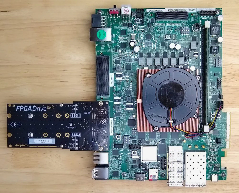
The rest of this post is for anyone who is trying to create their own design with the QDMA in root port mode. I will write about what we found was important in getting everything to work in Vivado and PetaLinux.
If you’ve read any of my other posts on connecting NVMe SSDs to FPGAs, you might already be familiar with the XDMA, which is the IP that we would normally use for PCIe on Zynq UltraScale+ devices. On the Versal devices we need the QDMA Subsystem for PCIe. Interesting to note that the QDMA doesn’t wrap the gigabit transceivers and PCIe block into the same IP (as did the XDMA), instead you need to include them separately in your block design and make the interconnections. There are way too many connections to write about in this post so if you want to know more details, I suggest that you clone the Git repo, build the Vivado project and checkout the block design.
There are three QDMA address assignments to make in the Vivado design and the addresses/sizes you choose can be important.
This is the main configuration interface of the QDMA core. Important points:
0x8000_0000, 0x4_0000_0000, 0x5_0000_0000, these will all work for this interface)This interface provides access to the Bridge register space and the DMA register space. Important points:
It can be connected to the M_AXI_FPD or the M_AXI_LPD interfaces through a SmartConnect IP
It must be mapped to a 32-bit address (eg. 0x8000_0000, 0xB000_0000, etc) - it will not work at higher address ranges. If you
assign it to a higher address range (eg. 0x4_0000_0000), then the BARs do not get assigned during the PCIe initialization.
The below is an example boot log when the S_AXI_LITE_CSR is assigned to 0x4_0000_0000 - the BAR assignment just doesn’t happen.
[    4.708488] xilinx-xdma-pcie 400000000.qdma: host bridge /amba_pl@0/qdma@a8000000 ranges:
[    4.716743] xilinx-xdma-pcie 400000000.qdma:   No bus range found for /amba_pl@0/qdma@a8000000, using [bus 00-ff]
[    4.727109] xilinx-xdma-pcie 400000000.qdma:      MEM 0x00a8000000..0x00abffffff -> 0x00a8000000
[    4.736067] xilinx-xdma-pcie 400000000.qdma: PCIe Link is UP
[    4.741869] xilinx-xdma-pcie 400000000.qdma: PCI host bridge to bus 0000:00
[    4.748886] pci_bus 0000:00: root bus resource [bus 00-ff]
[    4.754413] pci_bus 0000:00: root bus resource [mem 0xa8000000-0xabffffff]
<----------- BAR ASSIGNMENT NORMALLY HAPPENS HERE ------------->
The tools will assign this to a size of 256M but it can be given a size as small as 16K
This is the BAR interface. Here are the important points:
0x8000_0000, 0xB000_0000, etc) - it will not work at higher address ranges. If you
assign it to a higher address range (eg. 0x4_0000_0000), then we get the error message
non-prefetchable memory resource required and then the BARs of the SSD and bridge fail to get mapped. The below is an example boot log when
the S_AXI_BRIDGE is assigned to 0x4_3000_0000:[ 4.708959] xilinx-xdma-pcie 400000000.qdma: host bridge /amba_pl@0/qdma@b0000000 ranges:
[ 4.717216] xilinx-xdma-pcie 400000000.qdma: No bus range found for /amba_pl@0/qdma@b0000000, using [bus 00-ff]
[ 4.727584] xilinx-xdma-pcie 400000000.qdma: MEM 0x0430000000..0x043fffffff -> 0x0430000000
[ 4.736454] xilinx-xdma-pcie 400000000.qdma: non-prefetchable memory resource required
<-------------------- SKIPPING LINES FOR CLARITY ------------------------>
[ 4.809157] pci 0000:00:00.0: BAR 8: no space for [mem size 0x00100000]
[ 4.815817] pci 0000:00:00.0: BAR 8: failed to assign [mem size 0x00100000]
[ 4.822828] pci 0000:01:00.0: BAR 0: no space for [mem size 0x00004000 64bit]
[ 4.830015] pci 0000:01:00.0: BAR 0: failed to assign [mem size 0x00004000 64bit]Depending on which version of the tools you are using, you will need to correct the qdma_0 node of the automatically generated
device tree pl.dtsi (found in components/plnx_workspace/device-tree/device-tree/). You should do this by adding to the
system-user.dtsi file found in project-spec/meta-user/recipes-bsp/device-tree/files/.
ranges parameter.I can’t speak for other versions so if you’re using a version other than those I have mentioned above, I recommend that you just build the
PetaLinux project and then look through the automatically generated device tree pl.dtsi and compare it with the device tree below.
qdma_0: axi-pcie@400000000 {
	#address-cells = <3>;
	#interrupt-cells = <1>;
	#size-cells = <2>;
	clock-names = "user_clk_sd";
	clocks = <&misc_clk_0>;
	compatible = "xlnx,qdma-host-3.00";
	device_type = "pci";
	interrupt-map = <0 0 0 1 &psv_pcie_intc_0 1>, <0 0 0 2 &psv_pcie_intc_0 2>, <0 0 0 3 &psv_pcie_intc_0 3>, <0 0 0 4 &psv_pcie_intc_0 4>;
	interrupt-map-mask = <0 0 0 7>;
	interrupt-names = "misc", "msi0", "msi1";
	interrupt-parent = <&gic>;
	interrupts = <0 84 4 0 85 4 0 86 4>;
	ranges = <0x02000000 0x00000000 0xA8000000 0x0 0xA8000000 0x00000000 0x08000000>;
	reg = <0x0 0x80000000 0x0 0x4000>, <0x00000004 0x00000000 0x0 0x20000000>;
	reg-names = "breg", "cfg";
	psv_pcie_intc_0: interrupt-controller {
		#address-cells = <0>;
		#interrupt-cells = <1>;
		interrupt-controller ;
	};
};
Note that in the above example, the following address mappings were made in the Vivado design:
| Interface | Label | Address | Size |
|---|---|---|---|
| S_AXI_LITE | cfg | 0x4_0000_0000 | 256M |
| S_AXI_LITE_CSR | breg | 0x8000_0000 | 16K |
| S_AXI_BRIDGE | BAR0 | 0xA800_0000 | 128M |
All of the lines in the above device tree are required. Check the automatically generated device tree in pl.dtsi and add any missing or
incorrect parameters to the node in system-user.dtsi. Here is an example for correcting the compatible parameter in system-user.dtsi:
&qspi_0 {
	compatible = "xlnx,qdma-host-3.00";
};The compatible parameter is necessary for hooking the QDMA up with the correct driver. You must ensure that it is set
to "xlnx,qdma-host-3.00" as above and that the
QDMA Root port Linux driver patch has been applied (see next section
for more info).
The interrupt-map, interrupt-map-mask parameters and the interrupt-controller node should just be copied as they are in the example above.
If you don’t include them, you get this error message in the boot log: No PCIe Intc node found.
The interrupt-names parameter is essential and it must be set to "misc", "msi0", "msi1".
If it is not set correctly, you end up with the following error messages in the boot log:
[    4.744481] xilinx-xdma-pcie 400000000.qdma: IRQ misc not found
[    4.750447] xilinx-xdma-pcie 400000000.qdma: Unable to find misc IRQ line
[    4.757292] xilinx-xdma-pcie 400000000.qdma: Parsing DT failed
The interrupts parameter is correctly generated by the tools in version 2022.1 and 2023.2. You should not have to include
this in your system-user.dtsi. If you have connected the QDMA’s three interrupts to the Versal PL-to-PS interrupts, then
you can check your interrupt indicies with the table below:
| Pin | Index | Pin | Index |
|---|---|---|---|
| pl_ps_irq0 | 84 | pl_ps_irq8 | 92 |
| pl_ps_irq1 | 85 | pl_ps_irq9 | 93 |
| pl_ps_irq2 | 86 | pl_ps_irq10 | 94 |
| pl_ps_irq3 | 87 | pl_ps_irq11 | 95 |
| pl_ps_irq4 | 88 | pl_ps_irq12 | 96 |
| pl_ps_irq5 | 89 | pl_ps_irq13 | 97 |
| pl_ps_irq6 | 90 | pl_ps_irq14 | 98 |
| pl_ps_irq7 | 91 | pl_ps_irq15 | 99 |
The ranges parameter is critical and it is not correctly generated by version 2022.1 or 2023.2 of the tools. You will
have to override it as shown below:ranges = <0x02000000 0x00000000 <BAR address> 0x0 <BAR address> 0x00000000 <BAR size>>;
Without the correct ranges parameter, we were getting this kernel panic that occurred after the NVMe device is enabled:
[    3.871263] nvme nvme0: pci function 0000:01:00.0
[    3.876066] pci 0000:00:00.0: enabling device (0000 -> 0002)
[    3.881780] nvme 0000:01:00.0: enabling device (0000 -> 0002)
[    3.887579] SError Interrupt on CPU0, code 0x00000000bf000000 -- SError
[    3.887585] CPU: 0 PID: 20 Comm: kworker/u4:1 Not tainted 6.1.30-xilinx-v2023.2 #1
[    3.887590] Hardware name: Xilinx Versal vck190 Eval board revA (DT)
[    3.887593] Workqueue: nvme-reset-wq nvme_reset_work
[    3.887604] pstate: a0000005 (NzCv daif -PAN -UAO -TCO -DIT -SSBS BTYPE=--)
[    3.887609] pc : nvme_reset_work+0x174/0x11a0
[    3.887614] lr : nvme_reset_work+0x168/0x11a0
[    3.887618] sp : ffff80000981bca0
[    3.887619] x29: ffff80000981bca0 x28: 0000000000000000 x27: ffff05000022cb00
[    3.887626] x26: ffff05000135b618 x25: ffff05000135b000 x24: ffff05000111f0b0
[    3.887631] x23: 00000000fffffff4 x22: ffff05000111f000 x21: 0000000000000002
[    3.887637] x20: ffffffffffffffff x19: ffff05000135b210 x18: 0000000000000006
[    3.887642] x17: ffff8000095107c0 x16: 0000000053c185ff x15: ffff80000981b670
[    3.887647] x14: 0000000000000000 x13: ffff8000094a6170 x12: 0000000000000279
[    3.887653] x11: 00000000000000d3 x10: ffff8000094d2170 x9 : ffff8000094a6170
[    3.887658] x8 : 00000000fffff7ff x7 : ffff8000094d2170 x6 : 0000000000000001
[    3.887663] x5 : 0000000000000000 x4 : 0000000000000006 x3 : 0000000000000000
[    3.887667] x2 : 00000000fffffffe x1 : ffffffffffffffff x0 : 0000000000000000
[    3.887673] Kernel panic - not syncing: Asynchronous SError Interrupt
[    3.887676] CPU: 0 PID: 20 Comm: kworker/u4:1 Not tainted 6.1.30-xilinx-v2023.2 #1
[    3.887680] Hardware name: Xilinx Versal vck190 Eval board revA (DT)
[    3.887682] Workqueue: nvme-reset-wq nvme_reset_work
[    3.887686] Call trace:
[    3.887688]  dump_backtrace.part.0+0xc0/0xd0
[    3.887698]  show_stack+0x18/0x30
[    3.887704]  dump_stack_lvl+0x6c/0x88
[    3.887709]  dump_stack+0x18/0x34
[    3.887712]  panic+0x164/0x31c
[    3.887717]  add_taint+0x0/0xb0
[    3.887723]  arm64_serror_panic+0x6c/0x7c
[    3.887727]  do_serror+0x28/0x70
[    3.887730]  el1h_64_error_handler+0x30/0x4c
[    3.887734]  el1h_64_error+0x64/0x68
[    3.887738]  nvme_reset_work+0x174/0x11a0
[    3.887742]  process_one_work+0x1fc/0x380
[    3.887748]  worker_thread+0x74/0x4b0
[    3.887752]  kthread+0xd8/0xdc
[    3.887756]  ret_from_fork+0x10/0x20
[    3.887761] SMP: stopping secondary CPUs
[    3.887765] Kernel Offset: disabled
[    3.887766] CPU features: 0x40000,40048108,0000420b
[    3.887769] Memory Limit: none
[    4.102066] ---[ end Kernel panic - not syncing: Asynchronous SError Interrupt ]---
The reg parameter was generated correctly by version 2023.2 of the tools, but not 2022.1. It needs to have the
addresses of the S_AXI_LITE (cfg) and S_AXI_LITE_CSM (breg) interfaces. The order that the addresses are listed in must
match the order of their labels in the reg-names parameter.
The reg-names parameter is used by the QDMA Linux driver to differentiate between the two configuration interfaces.
In version 2022.1 of the tools, the order is important because of how the driver was written. In that
version, you need to put breg before cfg, because the former is referenced in the driver code by it’s index, not
by it’s name. In version 2023.2 this problem seems to have been fixed, but it is still critical to use both labels
and to have their order match that of their corresponding addresses in the reg parameter.
For versions 2021.1 to 2023.2, the QDMA Linux driver needs to be patched to work in root port mode. The patch is described and provided on Answer record 76647. Note that at the time of writing, there is no patch for version 2023.2, but I’ve ported one that you can get here.
If you do not apply the patch, the QDMA does not get attached to any driver and so you will not see the PCIe initialization when PetaLinux boots.
The DDR Address Region 1 must be disabled in the AXI NoC that connects to the DDR memory. Without doing so, we were getting the following errors from the NVMe driver:
[   64.629072] nvme nvme0: I/O 24 QID 0 timeout, disable controller
[   64.741024] nvme nvme0: Device shutdown incomplete; abort shutdown
[   64.747297] nvme nvme0: Identify Controller failed (-4)
[   64.752528] nvme nvme0: Removing after probe failure status: -5
I was never able to get a clear understanding of this problem, but the solution was suggested in a forum post. In the forum post, it is recommended to remove the upper 6GB of DDR memory by modifying the device tree. My experience was that this was not sufficient to stop the errors - it needed to be removed from the Vivado design. If anyone has an explanation for this problem, or a better solution, please let me know.
I feel the need to say thanks to a few of my industry contacts; developers who were particularly generous towards me with their time and knowledge while we worked on this ref design. When so many companies are being secretive, it’s refreshing to find people that are willing to share knowledge and experience for the benefit others. Thank you!