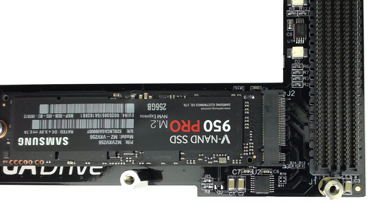
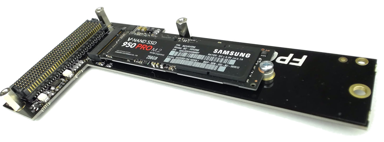
Let me introduce you to Opsero’s latest offering: FPGA Drive FMC, a new FPGA Mezzanine Card that allows you to connect an NVMe PCIe solid-state drive to your FPGA.
There’s got to be a better way. In the past, if you were developing an FPGA based product that needed a large amount of fast non-volatile storage, the best solution was to connect a SATA drive. Physical interfacing was pretty simple because all you needed was one gigabit transceiver. The downside however with SATA drives is that they require an IP core to implement the protocol layers between the host processor and the gigabit transceivers. This IP core can cost thousands of dollars and it uses up a lot of the FPGA resources, which all pushes up the total system cost.
The better solution is the new SSD technology based on the NVM express interface. NVMe is a new technology that is set to replace SATA as the most common way for connecting SSDs in personal computers. The new M.2 NVMe SSDs use a 4 lane PCI express interface, which can connect directly to one of the integrated blocks for PCI express that are available in most of the Series-7 FPGAs and the Zynq-7000.
Benefits. The most significant benefit to using this solution versus using a SATA or SAS drive, is that you don’t need the SATA or SAS IP core. This greatly simplifies the FPGA design, reduces development time and saves the customer thousands of dollars in IP costs. The second benefit to this solution is that NVMe is dramatically faster than SATA and SAS. This is mainly due to two things: a faster physical interface and a more efficient protocol stack. A 4-lane Gen2 PCI express link has more than 3 times the bandwidth of SATA 3.0. What’s more, NVMe has a more efficient protocol stack which was designed from the ground up to better exploit the potential of modern SSDs. Intel has shown that NVMe reduces latency overhead by more than 50%. And the knock out punch is this: all major Linux distributions now have NVMe driver in-box support, and that includes PetaLinux from version 2015.4 and up. So this means that NVMe drives can be used in a Linux OS running on a Microblaze in an FPGA, or on the Zynq ARM, and without even having to write custom drivers. If you want to see how, just check out these tutorials on the subject.
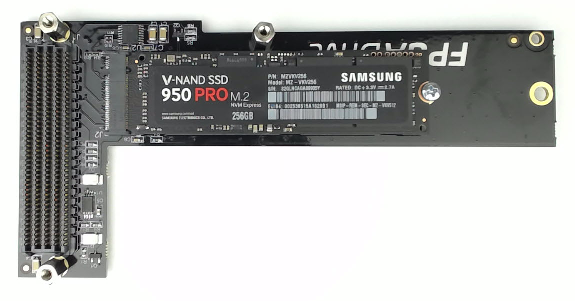
Features. So let’s get back to the FPGA Drive FMC and take a look at what’s on it:
- 1x M.2 socket M-keyed for PCIe SSDs
- 1x High-pin count FMC connector (mates with both LPC and HPC connectors)
- 1x 100MHz clock oscillator to supply a clock to the FPGA and the SSD
- 1x EEPROM to store the board’s FRU data (eg. serial number and power supply information)
- 2x LEDs: one for power good, one for the SSD activity
The board gets all of it’s power from the FMC connector, so there’s no power supply circuitry as there is on the PCIe edge connector version of the product. The board also has 4 mounting holes so that it can support all the 4 sizes of M.2 NVMe SSDs. The FMC uses two I/O signals, one for PERST (PCIe reset) driven by the FPGA, and one for PEDET (PCIe detect) driven by the SSD.
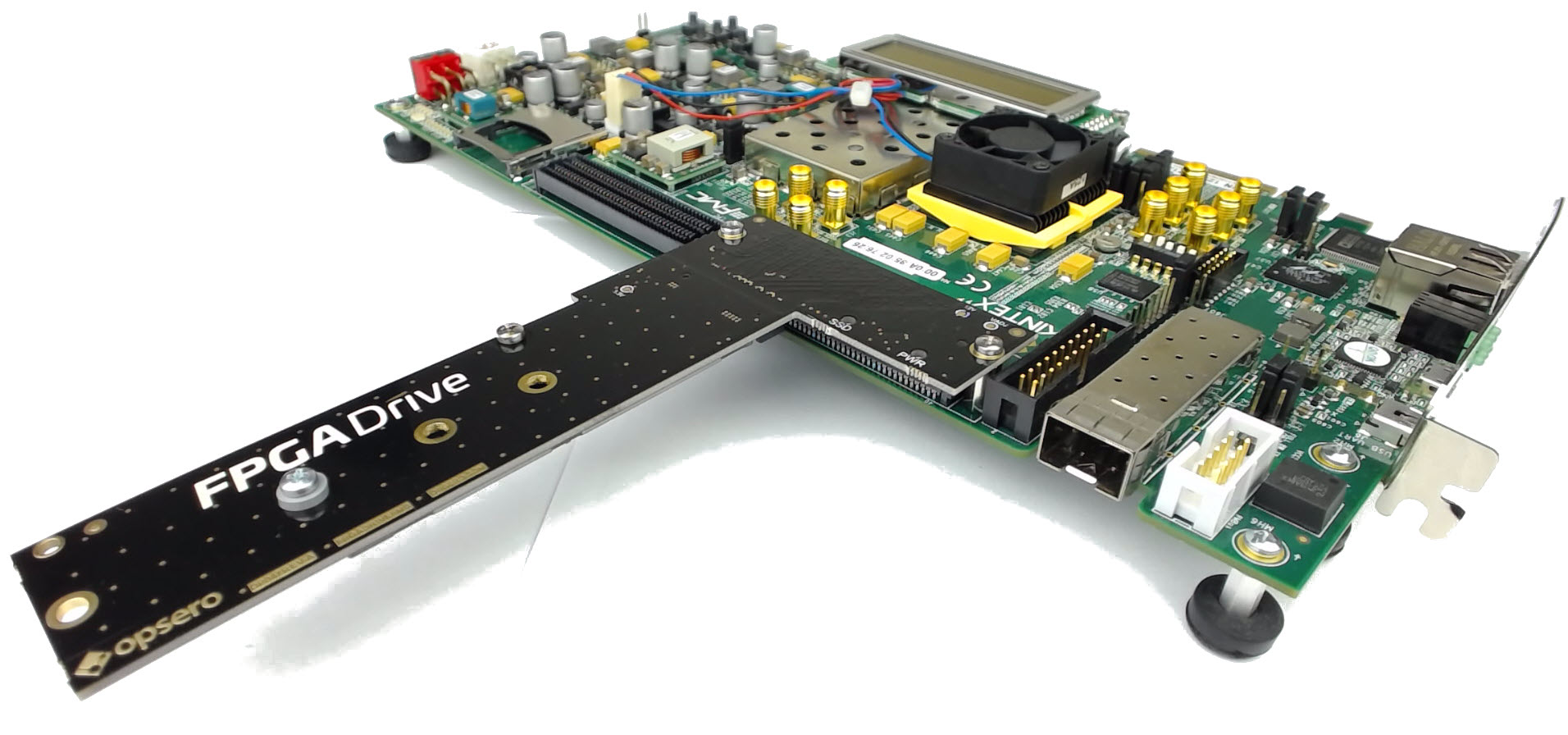
The images below show how the board interfaces with the PicoZed FMC Carrier Card V2 and the KC705.
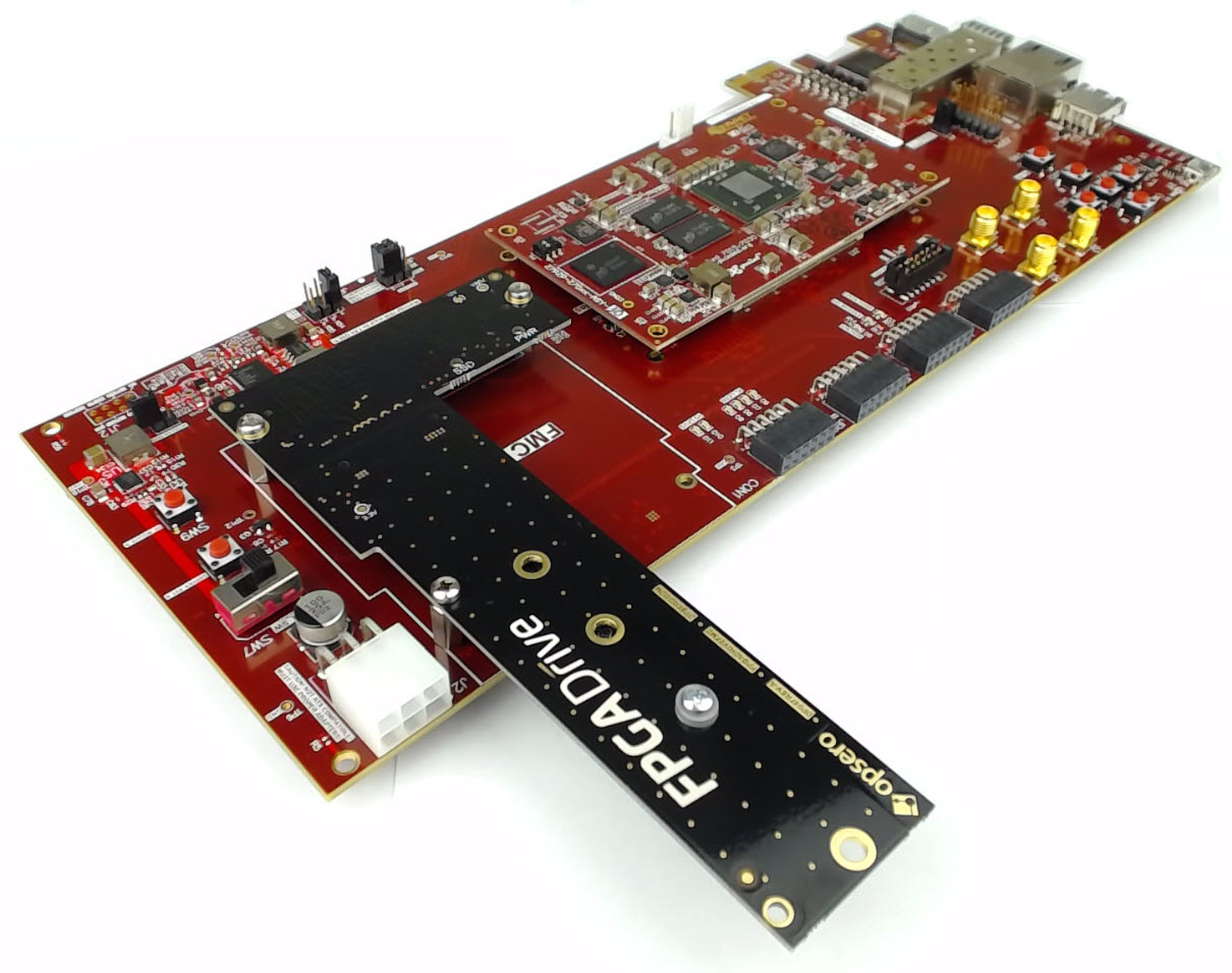
If you want more information about this product, please visit the product website at fpgadrive.com.
and Happy Canada Day!
