This is the first part of a three part tutorial series in which we will go through the steps to create a PCI Express Root Complex design in Vivado, with the goal of being able to connect a PCIe end-point to our FPGA. We will test the design on hardware by connecting a PCIe NVMe solid-state drive to our FPGA using the FPGA Drive adapter.
Part 1: Microblaze PCI Express Root Complex design in Vivado (this tutorial)
[Read More]FPGA Drive Board Bring-up
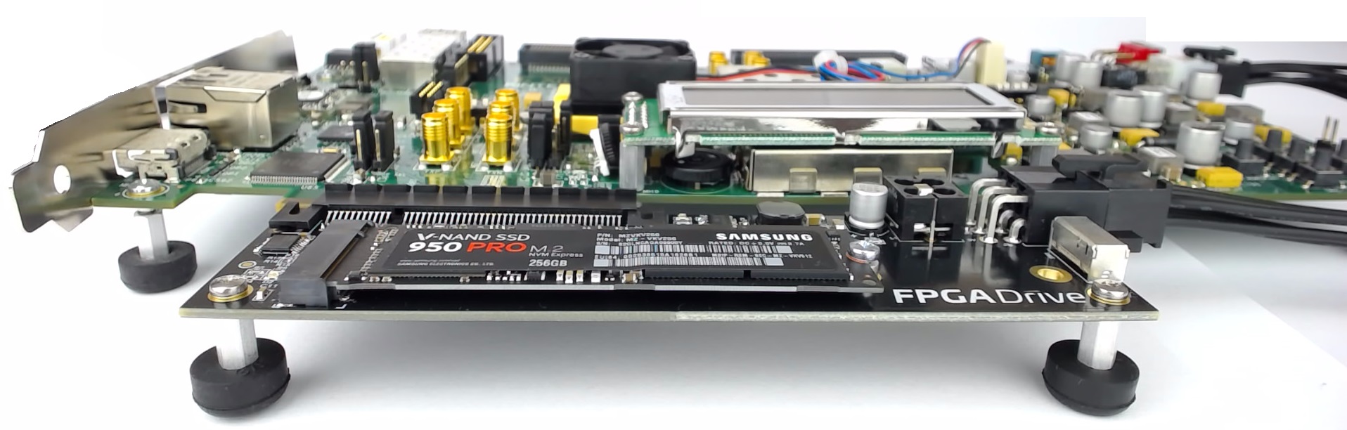
Bring-up of the first FPGA Drive with the Kintex-7 KC705 Evaluation board went nice and smoothly today. In the photo below you’ll see the KC705 and FPGA Drive adapter which is loaded with a Samsung V-NAND 950 Pro. The solid-state drive is an M.2 form factor, NVM Express, 4-lane PCI Express drive with 256GB of storage.
A little intro to NVM Express. NVM Express or NVMe is an interfacing specification for accessing SSDs over a PCI Express bus. By connecting the SSD over PCIe, it has a direct connection to the CPU which results in lower latency when compared to SATA drives, as well as increased throughput and potential for scaling (just add more lanes). PCIe SSDs can use the older AHCI interfacing standard, but due to the way that standard was designed, it can’t fully exploit the potential of modern SSDs. The NVMe specification was designed from the ground up to solve this problem.
[Read More]Unboxing Samsung V-NAND SSD 950 Pro M.2 NVM Express
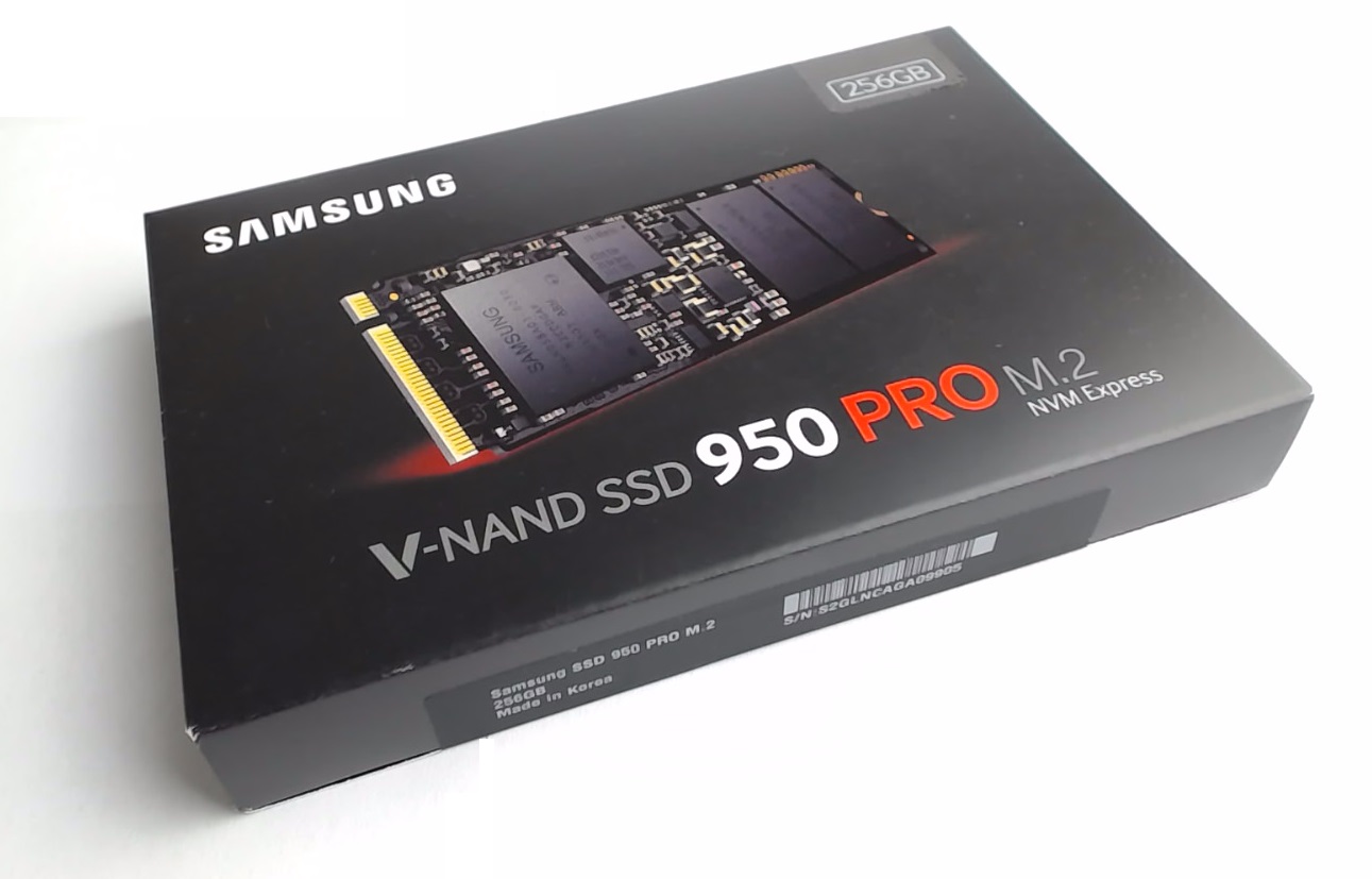
Very excited to be showing off my new Samsung SSD 950 in the M.2 form factor. This tiny solid-state drive has a PCI Express Gen3 x 4-lane interface for a more direct connection to the CPU which enables a much higher throughput than a SATA interface. According to Samsung:
It outperforms SATA SSDs by over 4.5 times in sequential read and by over 2.5 times in sequential write, delivering the speeds of 2,500 MB/s and 1,500 MB/s respectively.
[Read More]