Title here
Summary here
Tutorial on creating a Microblaze-based PCIe Root Complex design in Vivado to connect an NVMe SSD.
April 13, 201618 minutes

Bringing up the first FPGA Drive prototype with a Samsung NVMe SSD on the KC705 evaluation board.
March 31, 20164 minutes
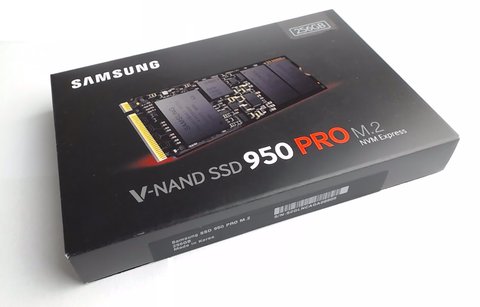
Unboxing the Samsung 950 Pro NVMe M.2 SSD for use with an FPGA via PCI Express.
February 13, 20161 minute