Title here
Summary here
A fresh approach to getting more from FMC
April 3, 202413 minutes

The FPGA Mezzanine Card standard ( VITA 57.1) has significantly enhanced the FPGA ecosystem by decoupling the FPGA board from the input/output components. Years ago, if you wanted to process samples from an ADC, you would buy an FPGA board with an on-board ADC. If you wanted to add a DAC, or upgrade the ADC, you would replace the entire board! The FMC innovation provided developers with choice, so that they could select the right FPGA for their specific I/O requirements. They could also swap-out their I/O cards as their needs changed or as upgrades or improvements became available.
Despite its advantages, the FMC standard has its limitations. Often, carrier boards can only host a single FMC card, challenging developers to find (or create) one FMC card that meets all of their I/O requirements. Even on dual FMC carriers, it can still be difficult to find the right FMC cards because some FMC slots are not fully connected, there can be incompatibility issues, or the requirements are just very specific and niche.
This is a problem that I have been wanting to tackle for years. For this reason, I’m excited to present Opsero’s latest product: The M.2 M-key Stack FMC. This is the first in a new range of FMCs that we’re calling: Stack FMC. The Stack FMC is Opsero’s answer to getting the most out of a single FMC connector while maximizing compatibility with carrier and mezzanine boards.
In this post I will present the M.2 M-key Stack FMC through a series of self-explanatory images and then I will discuss the Stack FMC concept that makes all this possible.
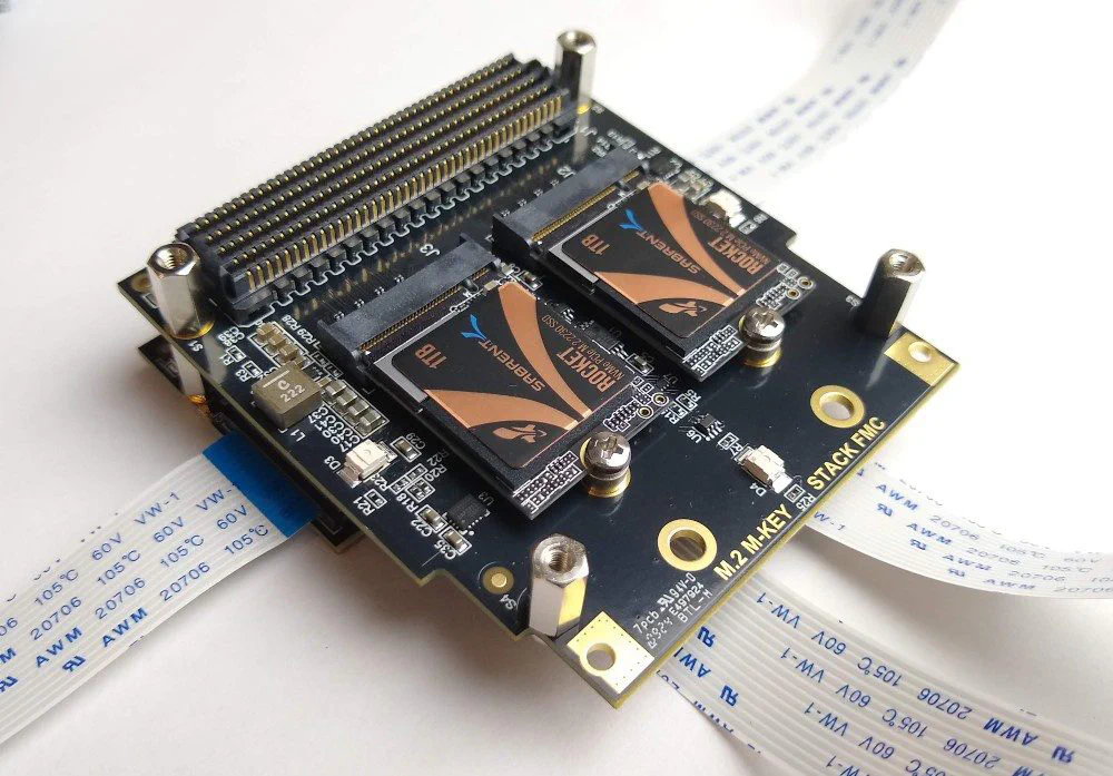
The M.2 M-key Stack FMC allows you to connect two M.2 M-key modules to an FPGA development board. There are many interesting M.2 M-key modules on the market but the most common ones are NVMe solid-state drives, so most applications for this product involve storing large quantities of data. If you’ve read my earlier post on multi-camera YOLOv5 you would know about another interesting M.2 module that can be used with this board: the Hailo-8 AI Accelerator. Offloading a AI workloads to an external engine can produce impressive results as you can read about in that post.
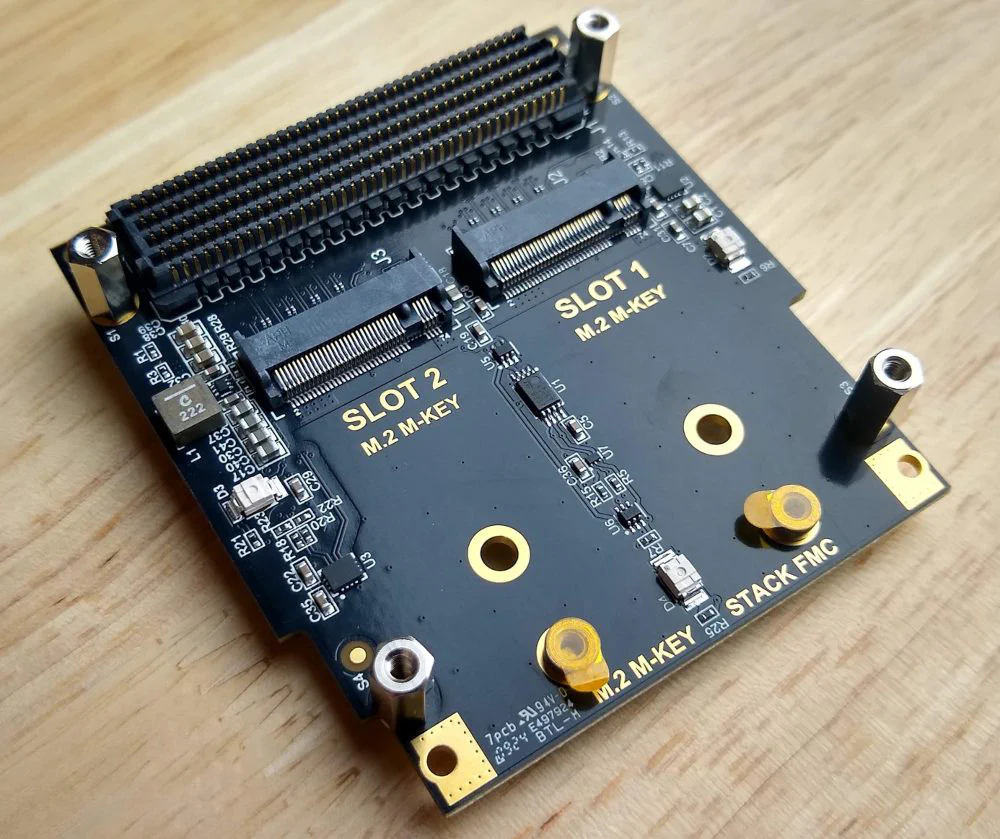
In the image below you can see the two M.2 slots and the mezzanine-side FMC connector.
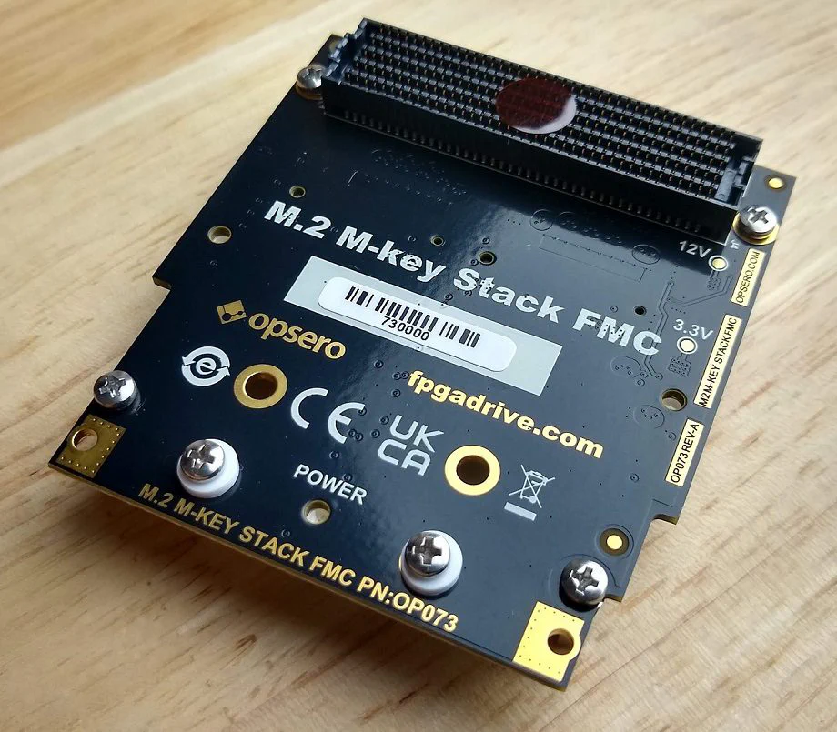
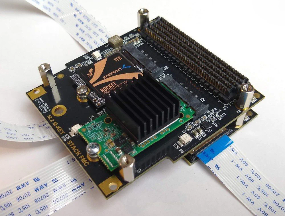
The image below shows the other side of the FMC card and the thing that differentiates this board from other Opsero FMC cards: a carrier-side FMC connector. This connector is used to mate with a second FMC card, such as the RPi Camera FMC or the Robust Ethernet FMC. Essentially, we can “stack” a second FMC card onto the M.2 M-key Stack FMC and get more out of a single FMC slot.
Any FMC card that does not require gigabit transceivers can be stacked on this product.
In the image below we see the M.2 M-key Stack FMC paired with the Robust Ethernet FMC. This combination enables four gigabit Ethernet ports and two 4-lane NVMe SSDs on your FPGA evaluation board from a single high pin count FMC connector. Other companies have stacked FMC cards together before, but what we’re trying to do with Stack FMC is to propose a standardized way of doing this, and importantly, one that is compatible with many existing FMC cards and carriers - not just Opsero FMCs.
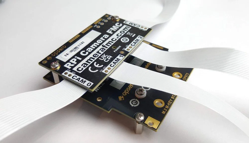
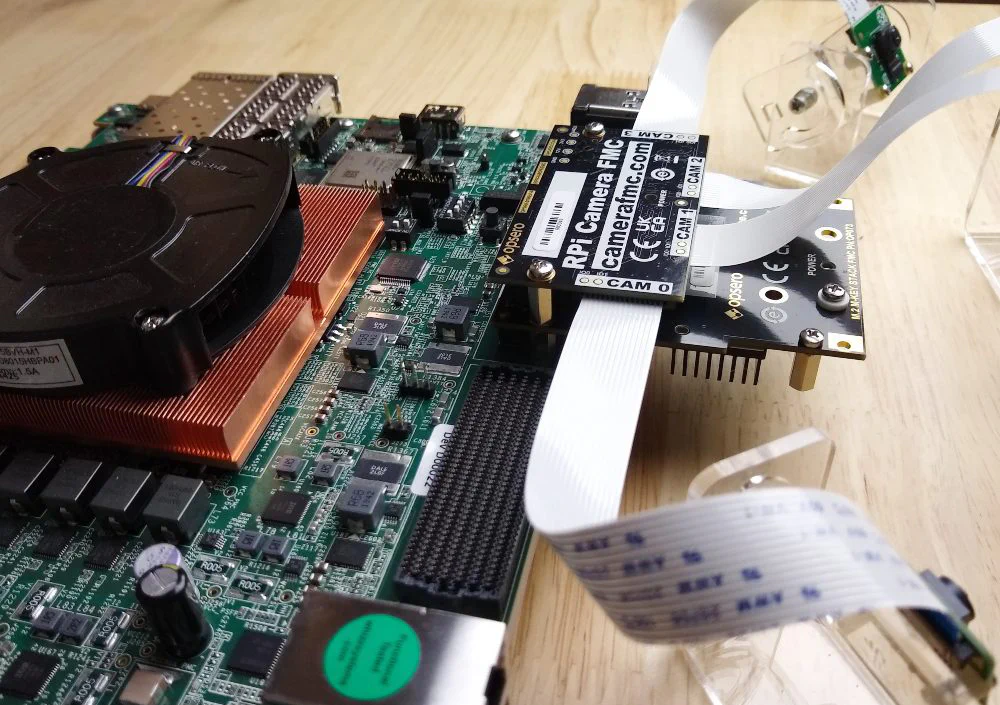
The image below shows the M.2 M-key Stack FMC when paired with the RPi Camera FMC. High capacity and non-volatile storage is a common requirement for image processing applications, making this pair extremely useful.
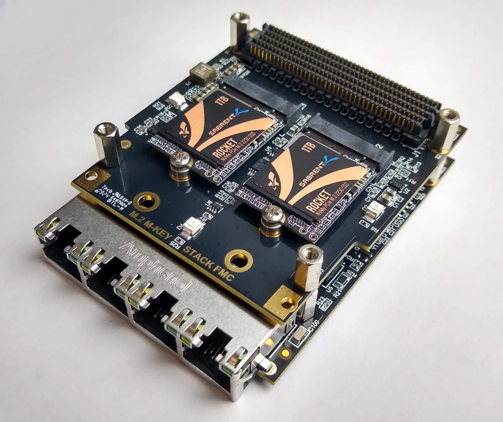
Flip it over and you can see two brand new 1TB Sabrent SSDs. These are in the M.2 2230 form factor (ie. 30mm long), but for those who need to use the more common 2280 form factor (80mm), we are designing an extension for this product - that’s what the golden tabs are for on the end of the board.
Swap out one of the SSDs for a Hailo-8 AI Accelerator (shown below) and you have another useful application for this pairing, combining AI acceleration, storage and multi-camera input through a single FMC connector. We’ve already released a reference design for doing this on the ZCU104, ZCU106, UltraZed-EV and PYNQ-ZU boards. You can download it here: Multi-camera YOLOv5 on the Zynq UltraScale+ and Hailo-8 AI Accelerator.
The image below shows this combination as it looks on the VCK190.
The M.2 M-key Stack FMC is only the first in a range of Stack FMCs that we plan to develop over the next few months. I’m hoping that it enables a wide range of applications that were previously out of reach for FPGA evaluation boards. If you would like to purchase the M.2 M-key Stack FMC, it should be available from Digi-Key by June.
In the rest of this post, I’m going to describe the Stack FMC concept for those who are interested to know more about it’s potential.
Most FMC cards don’t make use of all of the I/Os that are made available to them by the FMC carrier. An obvious solution to this problem is to forward all unused I/Os to a carrier-side FMC connector that is directly opposite the mezzanine-side FMC connector. This has been done before. I first encountered it in 2011 while working at Lyrtech, when we launched the Radio420X FMC. This design allowed us to stack two FMCs, effectively doubling the available RF channels. Stacking FMC cards in this way is a convenient solution because we don’t need to add long lossy traces between the carrier and the second FMC card, it’s easy to maintain trace length and impedance matching, and mechanically everything lines up where it needs to be.
With the M.2 M-key Stack FMC, we want to reintroduce this method for stacking two FMC cards together, however this time with a standardized approach to partitioning the I/Os and power supplies of a single FMC connector. The goals that we considered while designing this partitioning were: (1) compatibility: to maximize the number of existing FMC cards that could be used as the “second” mezzanine card; and (2) to respect the limits of the VITA 57.1 standard as much as possible (said another way: to break only the rules and limits that we absolutely need to, and all within the bounds of what is mechanically and electrically possible with typical FPGA development boards). Basically, we wanted to make a series of stackable FMC cards that can be used with FMC cards that are already on the market, not only Opsero FMCs.
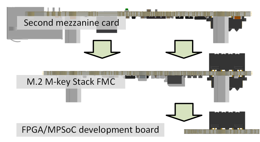
In a typical setup, the Stack FMC connects to the FPGA/MPSoC board, and a second FMC card connects to the carrier-side of the Stack FMC, as shown in the image below. This is the basic mechanical arrangement, and as you can probably tell, we already need to deviate from the VITA 57.1 standard in order to stack the boards in this way. We expect that this will not be possible on carriers that are housed in 1U rack mount enclosures. For this reason, we only really envisage these Stack FMCs being used on evaluation boards, where the mechanical constraints are relatively relaxed.
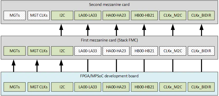
Without employing a sophisticated analog switching scheme, the I/Os need to be divided between the first and second mezzanine cards. I/Os that are used by one mezzanine card, are not available to the other. In a Stack FMC system:
This partitioning is illustrated by the image below.
Some of the advantages of this method for partitioning the I/Os are the following:
Some of the disadvantages are the following:
A standard FMC slot has a limited power budget and cannot be expected to power two FMC cards that both demand maximum utilization of all supplies. In order to ensure compatibility with a wide range of FMC cards, we cannot deprive the second FMC card slot of any of the supplies. Consequently, without the introduction of power from an external source or connector, sharing some of the FMC power supplies between the two FMC cards is inevitable. This creates a power budget problem. To get around this, we have to push the limits of the VITA 57.1 standard and ensure that we can justify it.
In a Stack FMC system:
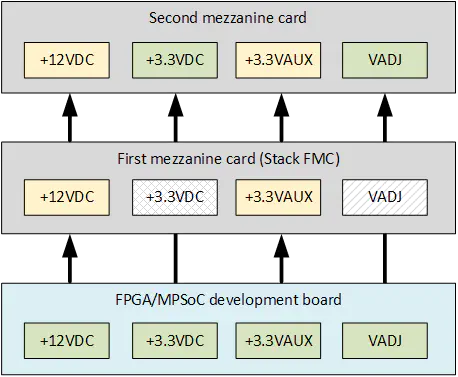
Sharing the +12VDC supply between the two FMC cards raises questions about the power budget, and thus needs further explanation. The FMC standard says that the carrier should be designed to provide at least 1A of current to the +12VDC pins of a single FMC slot. Put another way, an FMC card should not try to draw more than 1A from the FMC connector. A problem arises if the second FMC card requires all of the 1A current budget, and there is no budget left for the Stack FMC.
The reality is, however, that the real limit on the +12VDC supply is usually much greater than 1A, or it can be easily increased to match our needs. The reason is, most FPGA development boards are powered by a +12VDC supply, coming from an external 12VDC adapter. On these boards, this same power supply is routed directly to the FMC connector. This is the case for most of the AMD evaluation boards, such as the KC705, ZCU104 and VCK190. On such boards, the real current capability of the FMC’s +12VDC power supply is not limited by an on-board regulator or the VITA 57.1 spec but more so by the following:
| Real limits to FMC +12VDC supply for most eval boards | Solution |
|---|---|
| The 12V adapter used to power the FPGA evaluation board | Can be verified; in the worst case can be swapped for a larger adapter |
| The width and thickness of the traces that deliver the +12VDC supply to the FMC connector | Can be verified |
| The current rating of any diodes or protection circuitry used in the +12VDC path | Can be verified |
| The size and number of vias used in the +12VDC path | Can be verified |
| The current limit of the pins of the FMC connector | Rated 2.7A x 2 pins = 5.4A (ie. greater than required 2A) |
A Stack FMC will potentially draw another 1A from the +12VDC power supply, but with a simple verification of the carrier board, and power adapter, it can be determined beforehand whether or not the extra current draw is possible. Such a verification should be done for most FMC applications in any case. The way that I see this being managed in the future is, Opsero performs the verifications and releases a list of the FPGA evaluation boards that are able to supply the current for our range of Stack FMCs. If a bigger 12VDC adapter is required for any particular boards, we will specify one.
Regarding the +3.3VAUX supply, it is a low current supply (20mA) that is intended to power the on-board EEPROM. It is (allowed to be but not always) separate from the main +3.3VDC supply so that it can be enabled independently by the carrier for the purpose of identifying the connected FMC card, without powering up the entire board. Due to it’s purpose, this supply must be shared between both boards, however it’s power budget is not a concern because 20mA is more than enough to power the EEPROMs of two FMC boards. Furthermore, the real limit for this supply is much higher than 20mA on most evaluation boards.
In the case of the M.2 M-key Stack FMC, it has a buck converter to generate the +3.3VDC that is required by the M.2 modules. The buck converter is fed entirely by the +12VDC supply.
The I2C bus in the VITA 57.1 standard was intended for the FMC card’s EEPROM which stores information about the card including part number, manufacturer name and the I/O voltage that it expects to interface with (aka. VADJ). With Stack FMC, we add another purpose to the I2C bus: to allow for I/O expanders and other I2C devices to be used on the Stack FMC for general purpose I/O and other low-speed uses. These devices must be chosen such that they do not clash with the EEPROM’s I2C address.
The EEPROM identifies the connected FMC card, and also determines the VADJ voltage to be applied by the carrier board. Although the Stack FMC is indifferent to the VADJ voltage, it still requires an EEPROM for identification if it is used alone (without a second FMC). According to the standard, the EEPROM must use an I2C address that is determined by the GA0 and GA1 pins, and is given by the table below:
| A6 | A5 | A4 | A3 | A2 | A1 (GA0) | A0 (GA1) | Hexadecimal |
|---|---|---|---|---|---|---|---|
| 1 | 0 | 1 | 0 | 0 | 0 | 0 | 0x50 |
| 1 | 0 | 1 | 0 | 0 | 0 | 1 | 0x51 |
| 1 | 0 | 1 | 0 | 0 | 1 | 0 | 0x52 |
| 1 | 0 | 1 | 0 | 0 | 1 | 1 | 0x53 |
For most FPGA evaluation boards, GA0=0 and GA1=0, which corresponds to an I2C address of 0x50 for the EEPROM. In the case of a Stack FMC, there are potentially two EEPROMs on the same I2C bus: one on the Stack FMC and one on the second FMC. To avoid an address clash between these two EEPROMs, the Stack FMC must switch the address of it’s own EEPROM depending on the presence of a second FMC card. To achieve this, the Stack FMC uses an EEPROM with an external pin that can be driven to determine the A2 bit of it’s address. The Stack FMC uses the PRSNT_M2C_L signal of it’s carrier-side FMC connector to determine whether or not a second FMC is present. If a second FMC is present, the Stack FMC must set A2 = 1, thus changing the address of it’s EEPROM, for example from 0x50 to 0x54. In this way, when a second FMC is present, the carrier card will read the EEPROM of the second FMC and use it to determine the correct VADJ voltage to apply. Likewise, when no second FMC is present, the carrier board will read the EEPROM of the Stack FMC and apply the VADJ voltage requested by it.
The EEPROM of the Stack FMC will be programmed accept any VADJ voltage in the range of 1.2VDC to 3.3VDC.
The M.2 M-key Stack FMC uses an I/O expander to provide access to the M.2 module reset signals. By default, these reset signals are pulled high by pull-up resistors when the board is powered up, releasing the modules from reset. The I/O expander allows access to these signals if the application requires this level of control.
In the following weeks, I’ll be writing up a more detailed specification for Stack FMC and publishing it online. For now, if you want more information, I suggest you take a look at the documentation for the M.2 M-key Stack FMC and take a look at how we designed it.
As I mentioned, we have more Stack FMCs in the pipeline and I’m excited to share the details about them in the coming weeks. I think that this concept has the potential to enable a lot of applications on FPGA development boards that previously would have required custom hardware.