Device

Kintex®-7 XC7K325T-2FFG900C FPGA

Configuration

FPGA configuration is determined by DIP switch SW13.

Config mode 1 2 3 4 5
JTAG X X 1 0 1
Master BPI Note 4 Note 4 0 1 0
Quad SPI X X 0 0 1

Notes:

  1. X = don’t care
  2. 0 = OFF position
  3. 1 = ON position
  4. Switches 1 and 2 are A25 and A24 respectively and determine which of 4 bitstreams is booted from the Linear BPI flash

Processorless Ethernet: Part 3

State machine based Ethernet on FPGA

Processorless Ethernet: Part 3

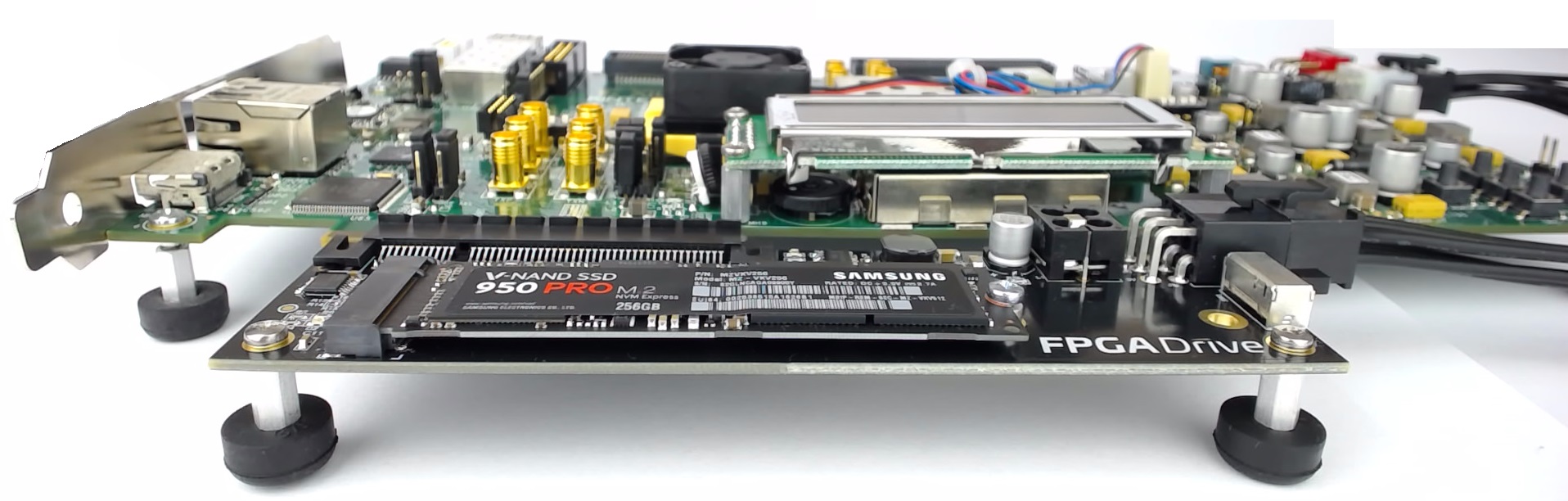
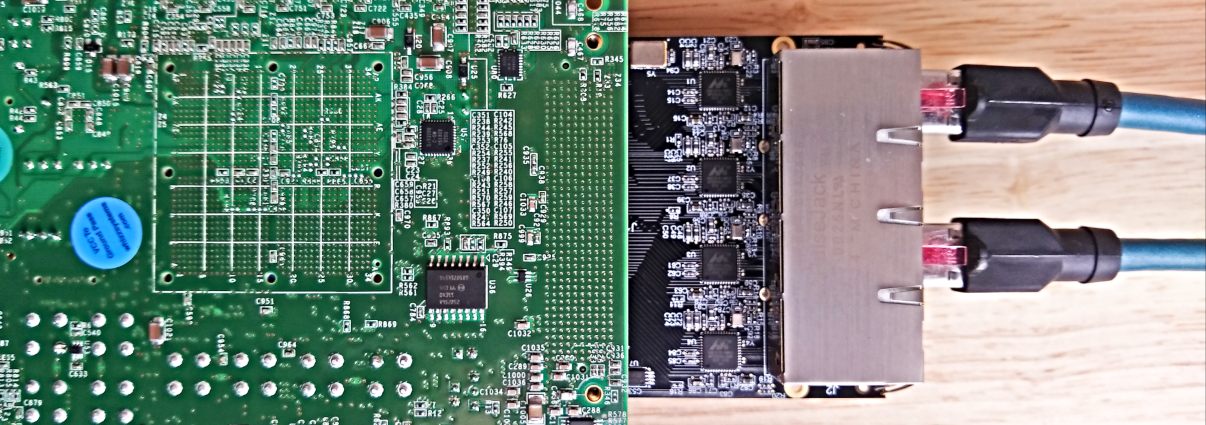
For those of you who want to experiment with processorless Ethernet on FPGAs, I’ve just released a 4-port example design that supports these Xilinx FPGA development boards:

Here’s the Git repo for the project: Processorless Ethernet on FPGA

Why processorless?

Pure hardware designs can trump software where the need for low latency and/or high throughput is greater than the need for flexibility and complexity (eg. the support of complex protocols). There are lots of applications that rely on hardware based packet processing to achieve their superior performance. High frequency trading platforms are often fed market pricing over multicast UDP, so their profitability is directly linked to their ability to process UDP with the lowest possible latency. Network security devices that monitor traffic usually need to be as transparent as possible while also being able to detect threats and take action with the lowest possible delay. Whatever your reason for processing Ethernet frames in the FPGA fabric, make sure that you consider both sides of the coin:

[Read More]

Processorless Ethernet: Part 2

Modularizing the TEMAC example design

Processorless Ethernet: Part 2
This article was written by Pablo Trujillo, an FPGA developer and consultant based in Valencia, Spain; a place that I happen to be very fond of, because of the many tapas bars and good eating/drinking to be done there. Pablo writes his own blog on FPGAs called Control Paths and he’s also a very active contributor to Hackster.io. In this article, Pablo explains how he has helped me to modularize the TEMAC example design that we looked at in an earlier post. The point of modularizing the design is to be able to easily extend it to the 4-ports of the Ethernet FMC, and it’s the first step in the development of a 4-port processorless reference design that supports multiple FPGA dev boards. I hope you enjoy reading this article and that it leads you to checkout more of his work. -Jeff

On one of the last posts we used the example design generated by Vivado for the tri_mode_ethernet_mac_ip, and we changed the port used by the example to one of the ports of the Ethernet FMC board. This time, we are going to modify the example design in order to make it easy to replicate the example project on the 4 ports of the FMC Ethernet. To do that, we will need to extract from the example the blocks that will be shared by all ports, and also modify the IP configuration in order to use the less different modules possible.

[Read More]

Driving Ethernet ports without a processor

How to do it on an FPGA and why

Driving Ethernet ports without a processor

Gigabit Ethernet can be a very useful medium for transferring data very quickly from one point to another. It’s low-cost, high-bandwidth, well established technology and the cabling is easily obtained and installed. In embedded applications however, the throughput of Ethernet links is often held back by one thing: the processor. When using an FPGA, we can relieve the processor significantly by offloading work to the FPGA fabric, but often the only way to exploit the full potential of a Gigabit Ethernet link is to do away with the processor altogether.

[Read More]

NVMe Host IP tested on FPGA Drive

NVMe Host IP tested on FPGA Drive

I’ve been totally overloaded with projects in the last couple months but I’m back with some really exciting news today. A few months back a company called IntelliProp, based in Colorado, released a NVMe Host Accelerator IP core for interfacing FPGAs with NVMe SSDs. This IP core allows reads and writes to be performed directly from the FPGA fabric, without the latency overhead of an operating system (read about the NVMe speed tests I did under PetaLinux). IntelliProp has tested their IP core with an FPGA Drive FMC loaded with a Samsung 950 Pro 256GB SSD and here are the results:

[Read More]
nvme 

Measuring the speed of an NVMe PCIe SSD in PetaLinux

With FPGA Drive we can connect an NVM Express SSD to an FPGA, but what kind of real-world read and write speeds can we achieve with an FPGA? The answer is: it depends. The R/W speed of an SSD depends as much on the SSD as it does on the system it’s connected to. If I connect my SSD to a 286, I can’t expect to get the same performance as when it’s connected to a Xeon. And depending on how it’s configured, the FPGA can be performing more like a Xeon or more like a 286. To get the highest performance from the SSD, the FPGA must be a pure hardware design, implementing NVMe protocol in RTL to minimize latency and maximize throughput. But that’s hard work, and not very flexible, which is why most people will opt for the less efficient configuration whereby the FPGA implements a microprocessor running an operating system. In this configuration, we typically wont be able to exploit the full bandwidth of NVMe SSDs because our processor is just not powerful enough.

[Read More]
nvme 

Connecting an SSD to an FPGA running PetaLinux

Connecting an SSD to an FPGA running PetaLinux

This is the final part of a three part tutorial series on creating a PCI Express Root Complex design in Vivado and connecting a PCIe NVMe solid-state drive to an FPGA.

In this final part of the tutorial series, we’ll start by testing our hardware with a stand-alone application that will verify the status of the PCIe link and perform enumeration of the PCIe end-points. We’ll then run PetaLinux on the FPGA and prepare our SSD for use under the operating system. PetaLinux will be built for our custom hardware using the PetaLinux SDK and the Vivado generated hardware description. Using Linux commands, we will then create a partition, a file system and a file on the solid-state drive.

[Read More]
nvme  pcie  ssd  popular 

Microblaze PCI Express Root Complex design in Vivado

This is the first part of a three part tutorial series in which we will go through the steps to create a PCI Express Root Complex design in Vivado, with the goal of being able to connect a PCIe end-point to our FPGA. We will test the design on hardware by connecting a PCIe NVMe solid-state drive to our FPGA using the FPGA Drive adapter.

Part 1: Microblaze PCI Express Root Complex design in Vivado (this tutorial)

[Read More]

FPGA Drive Board Bring-up

FPGA Drive Board Bring-up

Bring-up of the first FPGA Drive with the Kintex-7 KC705 Evaluation board went nice and smoothly today. In the photo below you’ll see the KC705 and FPGA Drive adapter which is loaded with a Samsung V-NAND 950 Pro. The solid-state drive is an M.2 form factor, NVM Express, 4-lane PCI Express drive with 256GB of storage.

A little intro to NVM Express. NVM Express or NVMe is an interfacing specification for accessing SSDs over a PCI Express bus. By connecting the SSD over PCIe, it has a direct connection to the CPU which results in lower latency when compared to SATA drives, as well as increased throughput and potential for scaling (just add more lanes). PCIe SSDs can use the older AHCI interfacing standard, but due to the way that standard was designed, it can’t fully exploit the potential of modern SSDs. The NVMe specification was designed from the ground up to solve this problem.

[Read More]
nvme 

Comparison of 7 Series FPGA boards for PCIe

Comparison of 7 Series FPGA boards for PCIe

One of my most common customer requests is to speed up execution of a software application using FPGA hardware acceleration. If the application runs on a PC or server, you can achieve impressive performance gains by using off-the-shelf FPGA development boards for PCI Express.

Here is a comparison of the available 7 Series FPGA boards for PCI Express applications:

AC701 Artix-7 KC705 Kintex-7 VC707 Virtex-7 VC709 Virtex-7
$1295 $1695 $3495 $4995
XC7A200T-2FBG676C XC7K325T-2FFG900C XC7VX485T-2FFG1761 XC7VX690T-2FFG1761C
4-lane Gen2 PCIe 8-lane Gen2 PCIe 8-lane Gen2 PCIe 8-lane Gen3 PCIe
1GB DDR3 SODIMM 1GB DDR3 SODIMM 1GB DDR3 SODIMM 4GB DDR3 SODIMM x2
8Kb EEPROM 8Kb EEPROM 8Kb EEPROM 1KB EEPROM
No BPI Flash 128MB BPI Flash 128MB BPI Flash 32MB BPI Flash
32MB Quad SPI 16MB Quad SPI 16MB Quad SPI No Quad SPI Flash
SD Card slot SD Card slot SD Card slot No SD
No LPC FMC 1x LPC FMC No LPC FMC No LPC FMC
1x HPC FMC (*) 1x HPC FMC (*) 2 x HPC FMC 1x HPC FMC (*)
1x SFP 1x SFP+ 1x SFP+ 4x SFP/SFP+
1GB Ethernet 1GB Ethernet 1Gb Ethernet No Ethernet
No USB No USB No USB No USB
UART over USB UART over USB UART over USB UART over USB
HDMI out HDMI out HDMI out No Video
XADC header XADC header AMS port No Analog
  • (*) Note: These HPC FMC connectors are only partially populated which means that they wont be able to support all standard FMCs.
  • There are many more FPGA boards for PCIe on the market, but I chose to limit the comparison to those that are more strongly supported by Xilinx.

The reason these types of boards are so useful in the hardware acceleration space is because PCI Express is the highest bandwidth, lowest latency link that you can have between a PC’s CPU and an external FPGA. There’s no use shipping off work to an FPGA if the time it takes the data to get there and back is more than the time saved through improved processing efficiency.

[Read More]