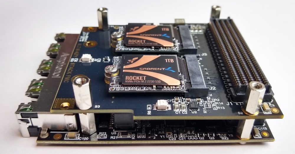
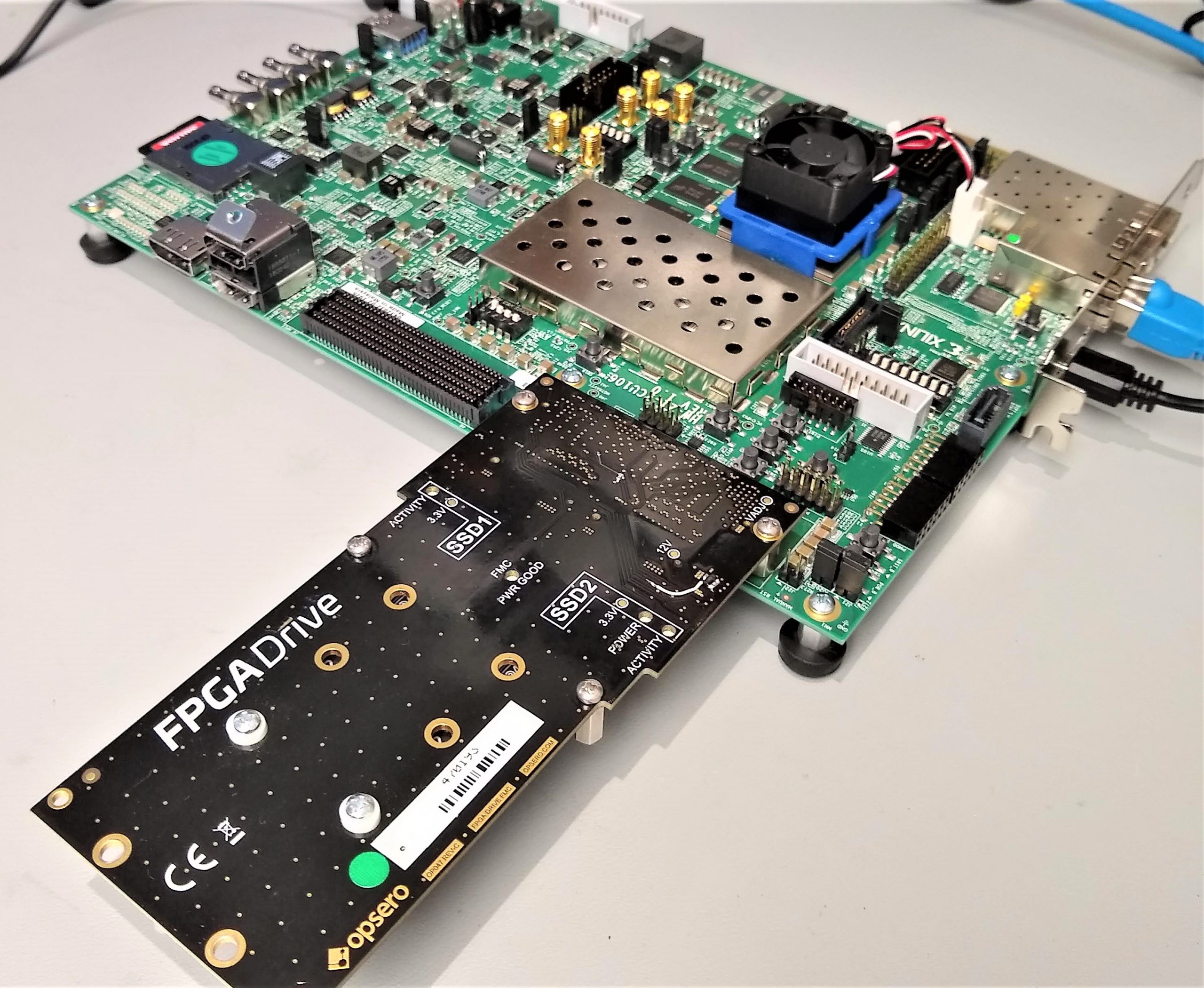
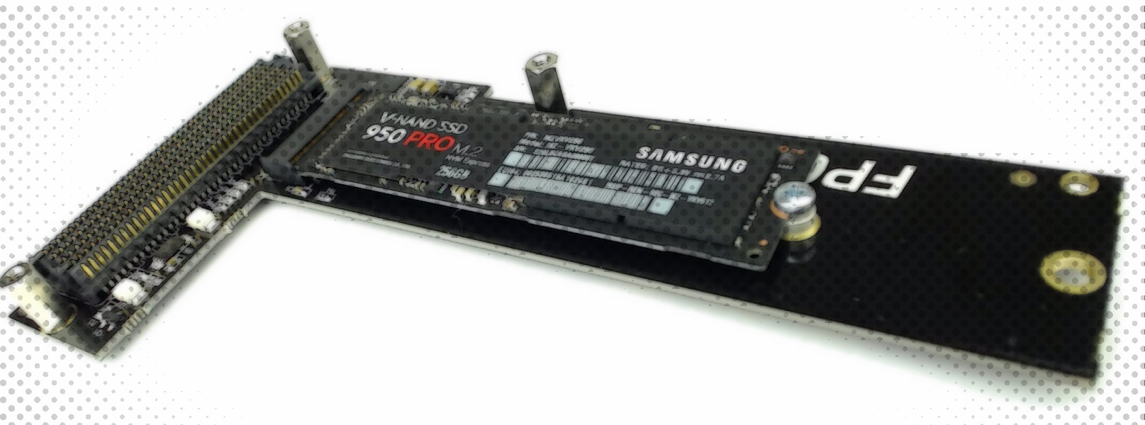
U.2 NVMe SSDs are the types of drives that are commonly used in enterprise servers and data centers. Compared to M.2 NVMe SSDs, which are more commonly found in consumer devices, U.2 drives are physically bigger, using the same form factor as the 2.5 inch SATA SSDs. The bigger form factor allows U.2 drives to consume more power and thus deliver higher sustained performance than their equivalent M.2 versions. This performance advantage is the reason why U.2 SSDs are becoming more popular in FPGA applications.
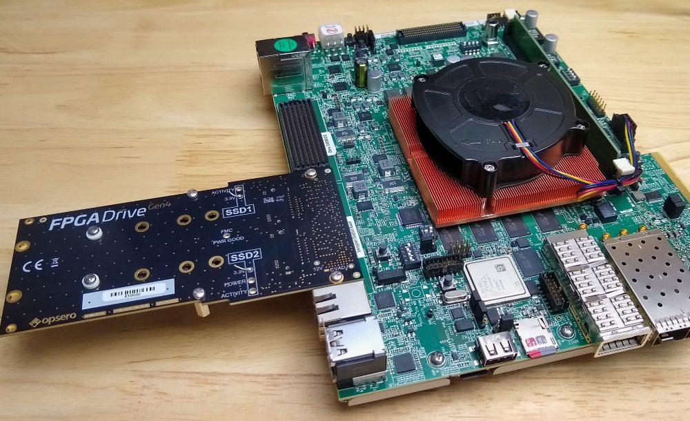
[Read More]Connecting U.2 NVMe SSDs to FPGAs
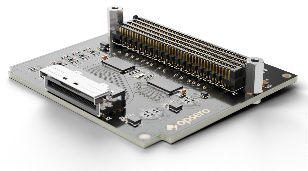
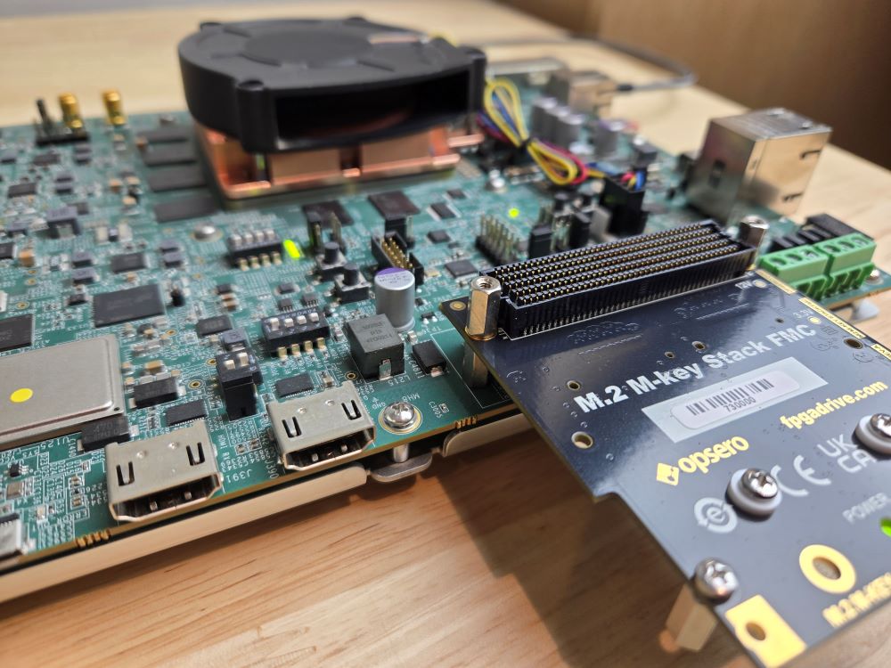
A solution using Mini Cool Edge IO and FMC