M2 SSD-to-FPGA adapter supports Gen4 PCIe

M2 SSD-to-FPGA adapter supports Gen4 PCIe

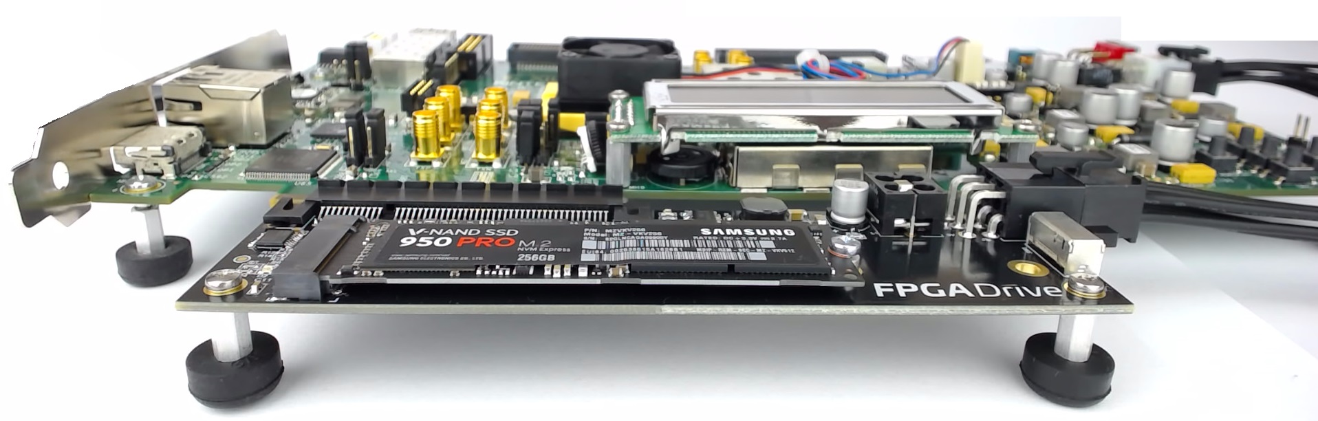
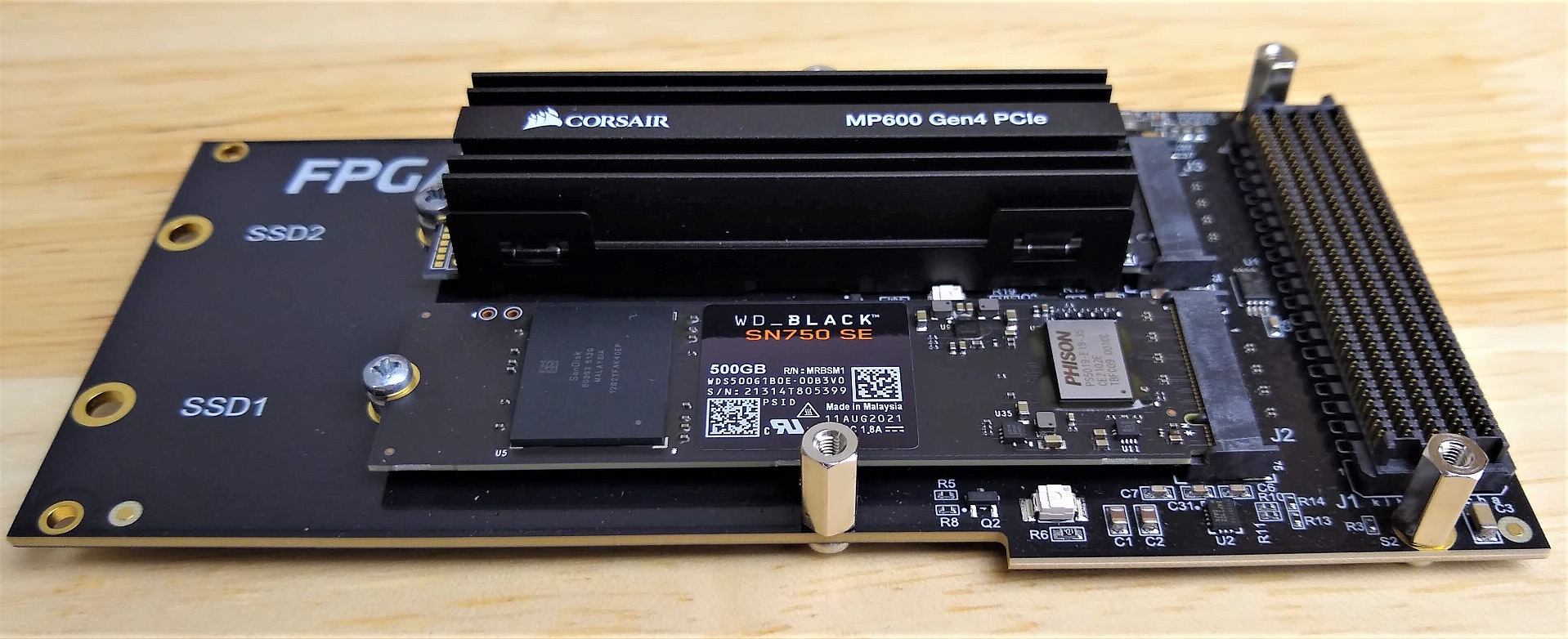
One of the projects I’ve been working on in the last few months has been upgrading our M2 SSD to FPGA adapter product (FPGA Drive FMC) to support the new Gen4 PCIe SSDs. It’s now available to buy so I thought that I would share some photos and write a bit about the changes that we made. The photos were taken with these two Gen4 PCIe SSDs:

  • Corsair Force Series MP600 1TB Gen4 PCIe NVMe M.2 SSD
  • WD_Black 500GB SN750 SE Gen4 PCIe NVMe M.2 SSD

Board material

Perhaps the most influential change to the PCB design was the change of board material. The original FPGA Drive FMC product was made with standard FR4 PCB laminate and it was designed to support up to PCIe Gen3 which operates at 8GHz. When we go up to PCIe Gen4, the signal frequency doubles to 16GHz, and we cross over a point where the losses of the FR4 laminate become a bit too high for operating reliable error-free serial links of a decent length.

[Read More]

Dev Board Quick References

Dev Board Quick References

In my work I have to use a lot of different FPGA and SoC dev boards, and when I switch from one to another it’s always a pain because I can never remember the little details like “What are the DIP settings to set the boot mode to SD card?” and “Where is the DIP switch for that?”. So my crutch for this has been to keep a little text file for each dev board containing the little useful details like:

[Read More]

Board bring-up: MYIR MYD-Y7Z010 Dev board

In this tutorial video, I bring-up the 3x Gigabit Ethernet ports on the MYD-Y7Z010 Development board from MYIR. Firstly, I create a Vivado design for this board, then I export it into the SDK and generate the echo server application for each of the 3 ports (note that the echo server application only supports one port at a time). At the end of the video, I test each of these designs on hardware and ensure that the ports are given an IP address via DHCP and that I can ping the port. I did this on the MYIR dev board but I hope that the tutorial can be of help to people bringing up Ethernet ports on other platforms or their own custom boards.

[Read More]
lwip  myir  zynq 

Artix-7 Arty Base Project

Here’s a base project for the Arty board based on the Artix-7 FPGA. The Arty is a nice little dev board because it’s low cost ($99 USD) but it’s still got enough power and connectivity to make it very useful. I really like the fact that the JTAG and UART are both accessed through the same USB connector, so I only need to connect one USB cable. I also like the fact that I can power it from the USB connector alone - provided I don’t connect too many power hungry PMods or an Arduino shield.

[Read More]

Getting Started with the MYIR Z-turn

In this video I create a simple Vivado design for the MYIR Z-turn Zynq SoM and we run a hello world application on it, followed by the lwIP echo server. We connect the Z-turn to a network, then we use “ping” and “telnet” to test the echo server from a PC that is connected to the same network.

[Read More]
zynq 

FPGA Drive Board Bring-up

FPGA Drive Board Bring-up

Bring-up of the first FPGA Drive with the Kintex-7 KC705 Evaluation board went nice and smoothly today. In the photo below you’ll see the KC705 and FPGA Drive adapter which is loaded with a Samsung V-NAND 950 Pro. The solid-state drive is an M.2 form factor, NVM Express, 4-lane PCI Express drive with 256GB of storage.

A little intro to NVM Express. NVM Express or NVMe is an interfacing specification for accessing SSDs over a PCI Express bus. By connecting the SSD over PCIe, it has a direct connection to the CPU which results in lower latency when compared to SATA drives, as well as increased throughput and potential for scaling (just add more lanes). PCIe SSDs can use the older AHCI interfacing standard, but due to the way that standard was designed, it can’t fully exploit the potential of modern SSDs. The NVMe specification was designed from the ground up to solve this problem.

[Read More]
nvme 

Creating a Base System for the Zynq in Vivado

Creating a Base System for the Zynq in Vivado

Tutorial Overview

In the ISE/EDK tools, we’d use the Base System Builder to generate a base project for a particular hardware platform. Now with Vivado, the process is a little different but we have more control in how things are setup and we still benefit from some powerful automation features. In this tutorial we’ll create a base design for the Zynq in Vivado and we’ll use the MicroZed board as the hardware platform.

[Read More]

Create an application using the Xilinx SDK

In the previous tutorial titled Creating a project using Base System Builder, we used Xilinx Platform Studio (EDK) to create a hardware design (bitstream) for the Zynq SoC. In this tutorial, we will complete the design by writing a software application to run on the ARM processor which is embedded in the Zynq SoC. Using the Xilinx SDK, we’ll create a simple application that will send the words “hello world” out of the serial port and into your PC serial console. In the next tutorials, we’ll write some applications that will interact with the peripherals we defined in the EDK project.

[Read More]
zynq 

Creating a project using the Base System Builder

I know I’ve gone through the Base System Builder many times before but I’m writing a few more advanced tutorials for version 14.7 and they all need a starting point. So in this post we will use the handy Base System Builder of the Xilinx Platform Studio (EDK) to put together a simple project for the ZC706 evaluation board.

Requirements

You will need the following :

  • Xilinx ISE Design Suite 14.7

Create the Project

Follow these steps to create the project:

[Read More]